Semiconductor device

a technology of semiconductor devices and semiconductors, applied in the direction of semiconductor devices, basic electric elements, electrical appliances, etc., can solve the problems of reducing the aperture ratio of a pixel and degrading the display quality of an image, and achieve the effect of increasing the charge capacity and improving the aperture ratio

Active Publication Date: 2016-01-26
SEMICON ENERGY LAB CO LTD
View PDF161 Cites 13 Cited by
  • Summary
  • Abstract
  • Description
  • Claims
  • Application Information

AI Technical Summary

Benefits of technology

[0011]As the capacitance of a capacitor is increased, a period in which the alignment of liquid crystal molecules of a liquid crystal element can be kept constant in the state where an electric field is applied can be made longer. When the period can be made longer in a display device which displays a still image, the number of times of rewriting image data can be reduced, leading to a reduction in power consumption.
[0019]When the nitride insulating film is in contact with the semiconductor film in the capacitor as described above, a step of adding an element which increases the conductivity to the semiconductor film by an ion implantation method, an ion doping method, or the like can be skipped; therefore, the yield of the semiconductor device can be improved and the manufacturing cost thereof can be reduced.
[0021]With the above structure, the capacitor transmits light and thus can be formed large (in a large area) in a region except a portion where the transistor in a pixel is formed. For this reason, the semiconductor device can have charge capacity increased while the aperture ratio is improved. As a result, the semiconductor device can have an excellent display quality.
[0024]With the above structure, one of or both nitrogen and hydrogen can be prevented from diffusing into the oxide semiconductor film as the semiconductor film of the transistor, so that variations in the electrical characteristics of the transistor can be suppressed.
[0026]The other electrode of the capacitor is electrically connected to the capacitor line. The capacitor line connected to the other electrode of the capacitor can be provided partly in contact with the electrode along the outer periphery thereof. In this manner, contact resistance between the electrode and the capacitor line can be reduced, so that charge can be efficiently supplied to the capacitor.
[0031]According to one embodiment of the present invention, a semiconductor device including a capacitor whose charge capacity is increased while the aperture ratio is improved can be provided.

Problems solved by technology

However, when the area of a light-blocking conductive film is increased in order to increase the area of a portion where a pair of electrodes overlap with each other, the aperture ratio of a pixel is lowered and thus display quality of an image is degraded.

Method used


Image

  • Semiconductor device
  • Semiconductor device
  • Semiconductor device

Examples


embodiment 1

[0056]In this embodiment, a semiconductor device of one embodiment of the present invention will be described with reference to drawings. Note that in this embodiment, a semiconductor device of one embodiment of the present invention is described taking a liquid crystal display device as an example.

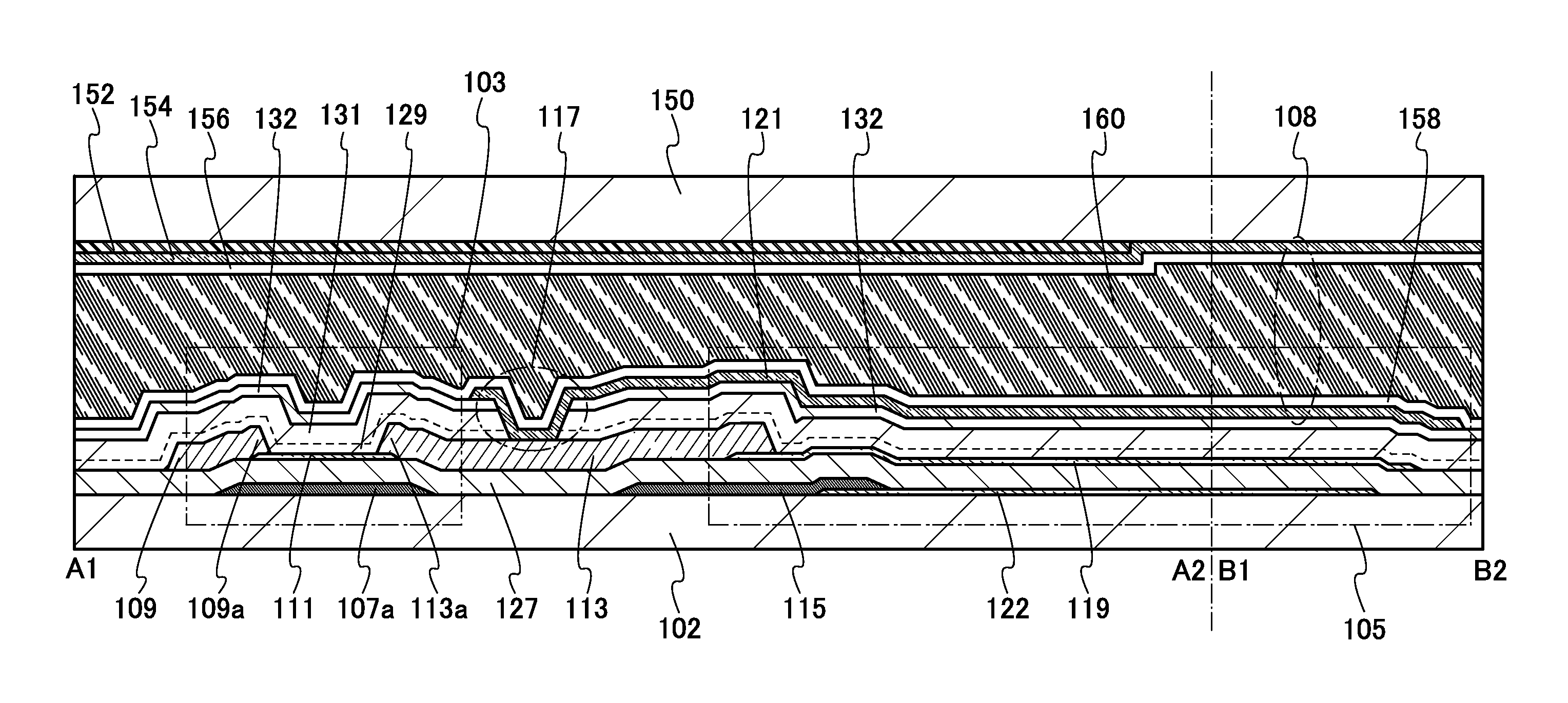
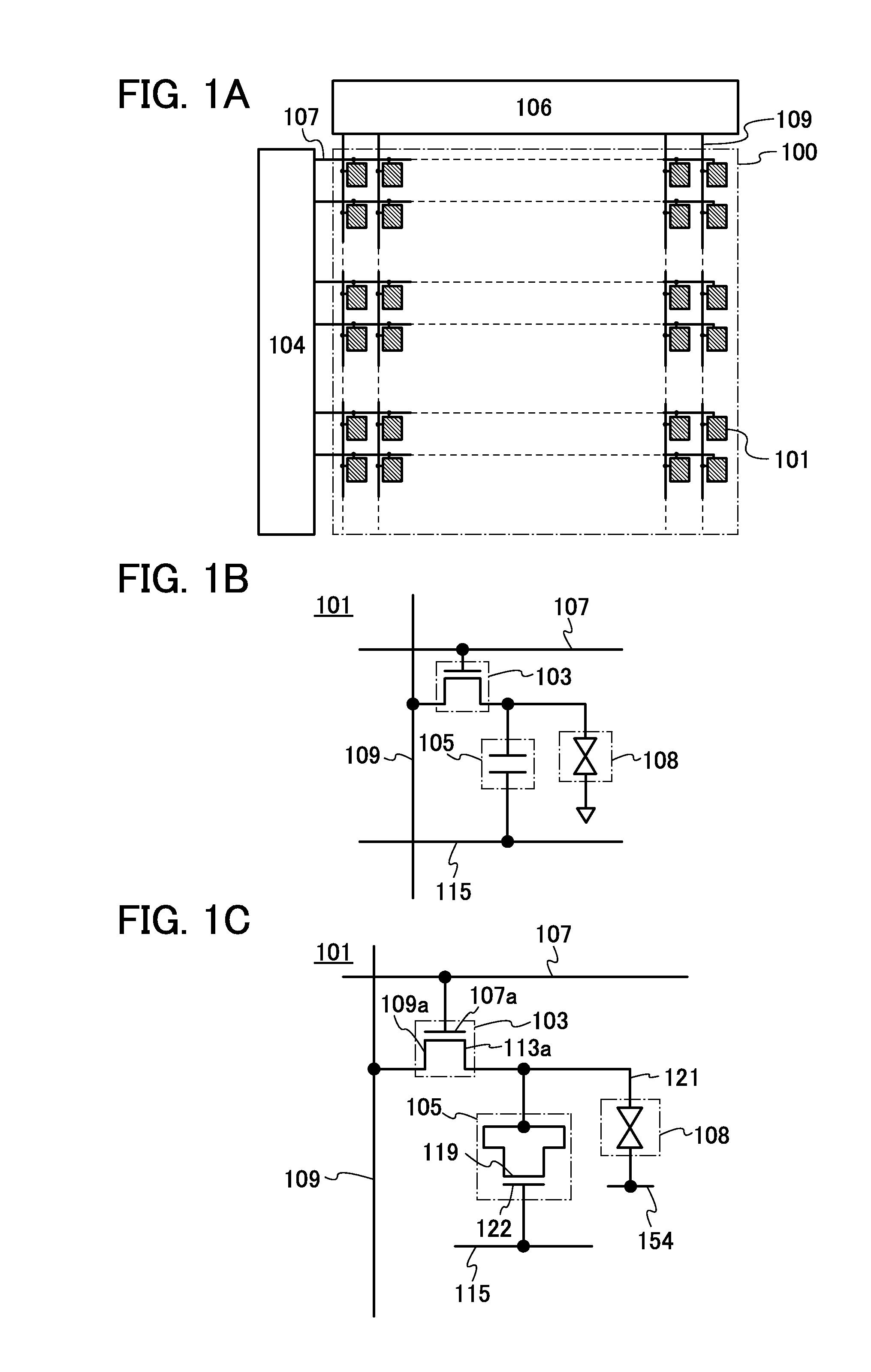
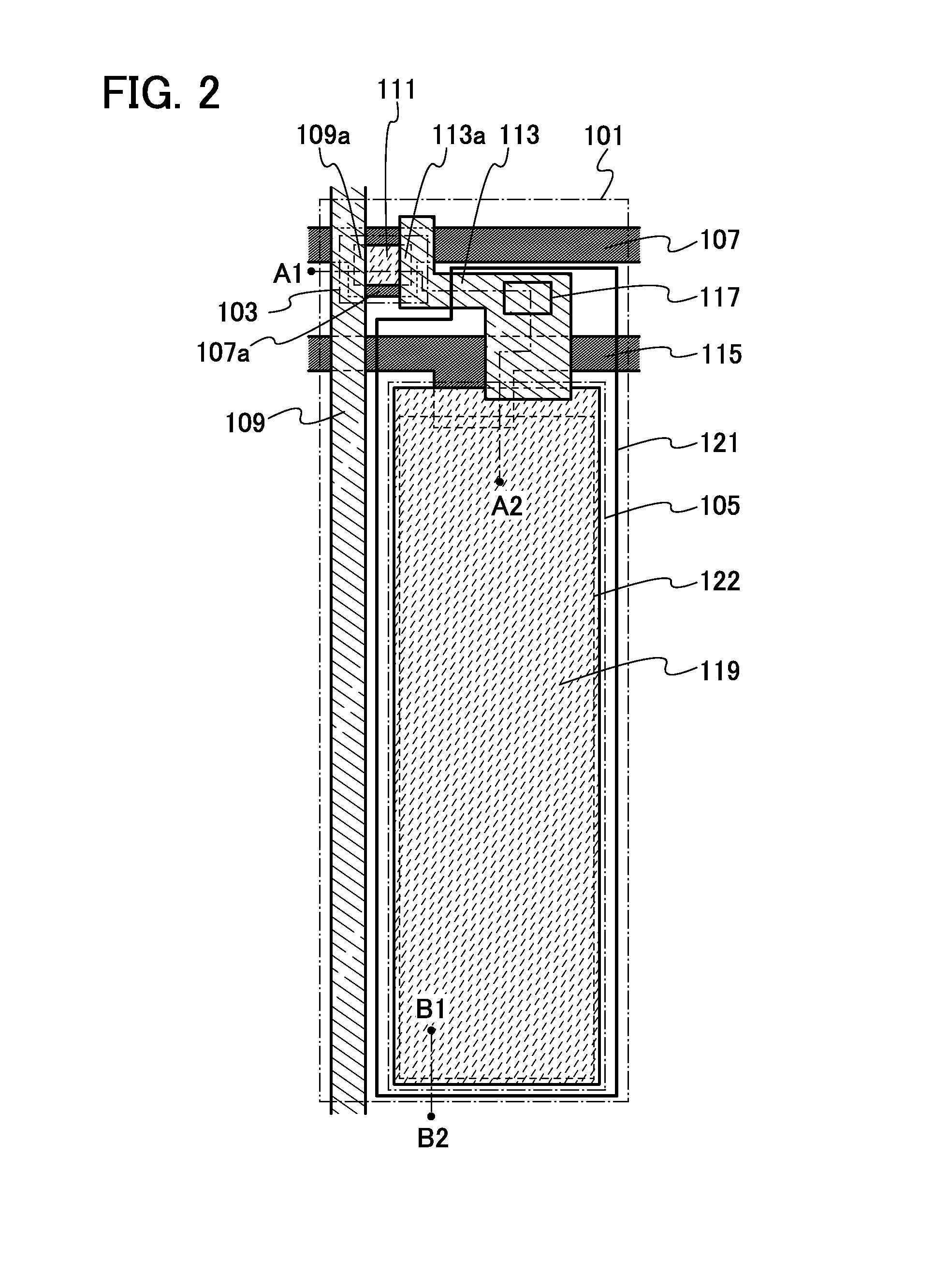
[0057]FIG. 1A illustrates an example of a structure of a semiconductor device. The semiconductor device in FIG. 1A includes a pixel portion 100, a scan line driver circuit 104, a signal line driver circuit 106, m scan lines 107 which are arranged in parallel or substantially in parallel and whose potentials are controlled by the scan line driver circuit 104, and n signal lines 109 which are arranged in parallel or substantially in parallel and whose potentials are controlled by the signal line driver circuit 106. Further, the pixel portion 100 includes a plurality of pixels 101 arranged in a matrix. Furthermore, capacitor lines 115 (not illustrated in FIG. 1A) arranged in parallel or subs...

modification example 1

[0169]In the semiconductor device of one embodiment of the present invention, the shape of a transistor provided in a pixel is not limited to the shape of the transistor illustrated in FIG. 2 and FIG. 3 and can be changed as appropriate. For example, as illustrated in FIG. 6, in a pixel 151, a transistor 153 may be different from the transistor 103 in that a source electrode included in the signal line 109 has a U shape (or a C shape, a square-bracket-like shape, or a horseshoe shape) which partly surrounds the conductive film 113 functioning as a drain electrode. With such a shape, a sufficient channel width can be ensured even when the area of the transistor is small, and accordingly, the amount of drain current flowing at the time of conduction of the transistor (also referred to as an on-state current) can be increased. The structure of the pixel 151 in FIG. 6 is similar to that in FIG. 2, except for the transistor 153.

modification example 2

[0170]In the semiconductor device of one embodiment of the present invention, the shape of the capacitor line 115 connected to the electrode 122 which is one electrode of the capacitor 105 can be changed as appropriate. For example, the capacitor line 115 can be provided partly in contact with the electrode 122 along the outer periphery thereof in order to reduce contact resistance between the electrode 122 and the capacitor line 115.

[0171]A specific example of the structure will be described with reference to FIG. 7, FIG. 8, and FIG. 9. Note that only portions different from those in FIG. 2 and FIG. 3 are described here. FIG. 7 is a top view of a pixel 161 in this structure, and FIG. 8 is a cross-sectional view taken along dashed-dotted lines A1-A2 and B1-B2 in FIG. 7. FIG. 9 is a cross-sectional view taken along dashed-dotted line C1-C2 in FIG. 7.

[0172]In the pixel 161 in this structure, a capacitor line 167 is provided in contact with the electrode 122 along the outer periphery t...


PUM


Abstract

A semiconductor device in which charge capacity of a capacitor is increased without a reduction in aperture ratio is provided. In a transistor including a light-transmitting semiconductor film and a capacitor in which a dielectric film is provided between a pair of electrodes, the pair of electrodes and the dielectric film are formed using a light-transmitting material. A semiconductor film which is formed on the same surface as the semiconductor film of the transistor is used as one of the pair of electrodes. The dielectric film included in the capacitor is formed using a gate insulating film. The other of the pair of electrodes is formed using a light-transmitting semiconductor film or a light-transmitting conductive film.

Description

BACKGROUND OF THE INVENTION[0001]1. Field of the Invention[0002]The invention disclosed in this specification and the like relates to semiconductor devices.[0003]In this specification, a semiconductor device means all types of devices that can function by utilizing semiconductor characteristics, and a transistor, a semiconductor circuit, a memory device, an imaging device, a display device, an electro-optical device, an electronic device, and the like are all semiconductor devices.[0004]2. Description of the Related Art[0005]In recent years, flat panel displays such as liquid crystal displays (LCDs) have been widespread. In each of pixels provided in the row direction and the column direction in a display device such as a flat panel display, a transistor serving as a switching element, a liquid crystal element electrically connected to the transistor, and a capacitor connected to the liquid crystal element in parallel are provided.[0006]As a semiconductor material for forming a semi...

Claims


Application Information

Patent Timeline
Patent Type & Authority Patents(United States)
IPC IPC(8): H01L29/10H01L21/00H01L33/00H01L27/12
CPCH01L33/0041H01L27/1225H01L27/1255H01L2924/0002H01L2924/00
Inventor YAMAZAKI, SHUNPEI
Owner SEMICON ENERGY LAB CO LTD
Why Eureka
Try Eureka