Laminate structures having a hole surrounding a probe for propagating millimeter waves

a technology of millimeter wave and laminate structure, which is applied in the direction of laminate, electrical equipment, special surfaces, etc., can solve the problems of degrading radiation propagation, affecting the efficiency and relatively complex structures of millimeter wave system on printed circuit board. achieve the effect of cost-effective construction

Active Publication Date: 2016-02-23
SIKLU COMM
View PDF15 Cites 3 Cited by
  • Summary
  • Abstract
  • Description
  • Claims
  • Application Information

AI Technical Summary

Benefits of technology

The patent describes a system and methods for injecting and guiding millimeter-waves through a printed circuit board. The system includes a PCB with first and second laminas, as well as a microstrip and a probe printed on the first lamina. There is also a hole in the PCB that forms a wall inside the board and conductive plating applied on parts of the wall that do not directly surround the probe. The system can radiate millimeter-waves from the probe and guide them through the hole and cage formed by the plated through-holes. The technical effects include higher quality and fewer components or stages of manufacturing, as well as easier and cost-effective construction.

Problems solved by technology

Some current millimeter-wave systems on a printed circuit board (“PCB”) have relatively complicated structures, with many components.
First, radiation propagation is degraded by the need for the radiation to propagate through the top lamina.
Second, the lower layers form a waveguide structure, but the source of radiation is separated from the waveguide structure by the thickness of the top lamina, and this separation also degrades the radiation propagation.
Third, these current systems are relatively difficult to manufacture.

Method used


Image

  • Laminate structures having a hole surrounding a probe for propagating millimeter waves
  • Laminate structures having a hole surrounding a probe for propagating millimeter waves
  • Laminate structures having a hole surrounding a probe for propagating millimeter waves

Examples


Embodiment Construction

[0088]It is noted that: (i) same features throughout the drawing figures will be denoted by the same reference label and are not necessarily described in detail in every drawing that they appear in, and (ii) a sequence of drawings may show different aspects of a single item, each aspect associated with various reference labels that may appear throughout the sequence, or may appear only in selected drawings of the sequence.

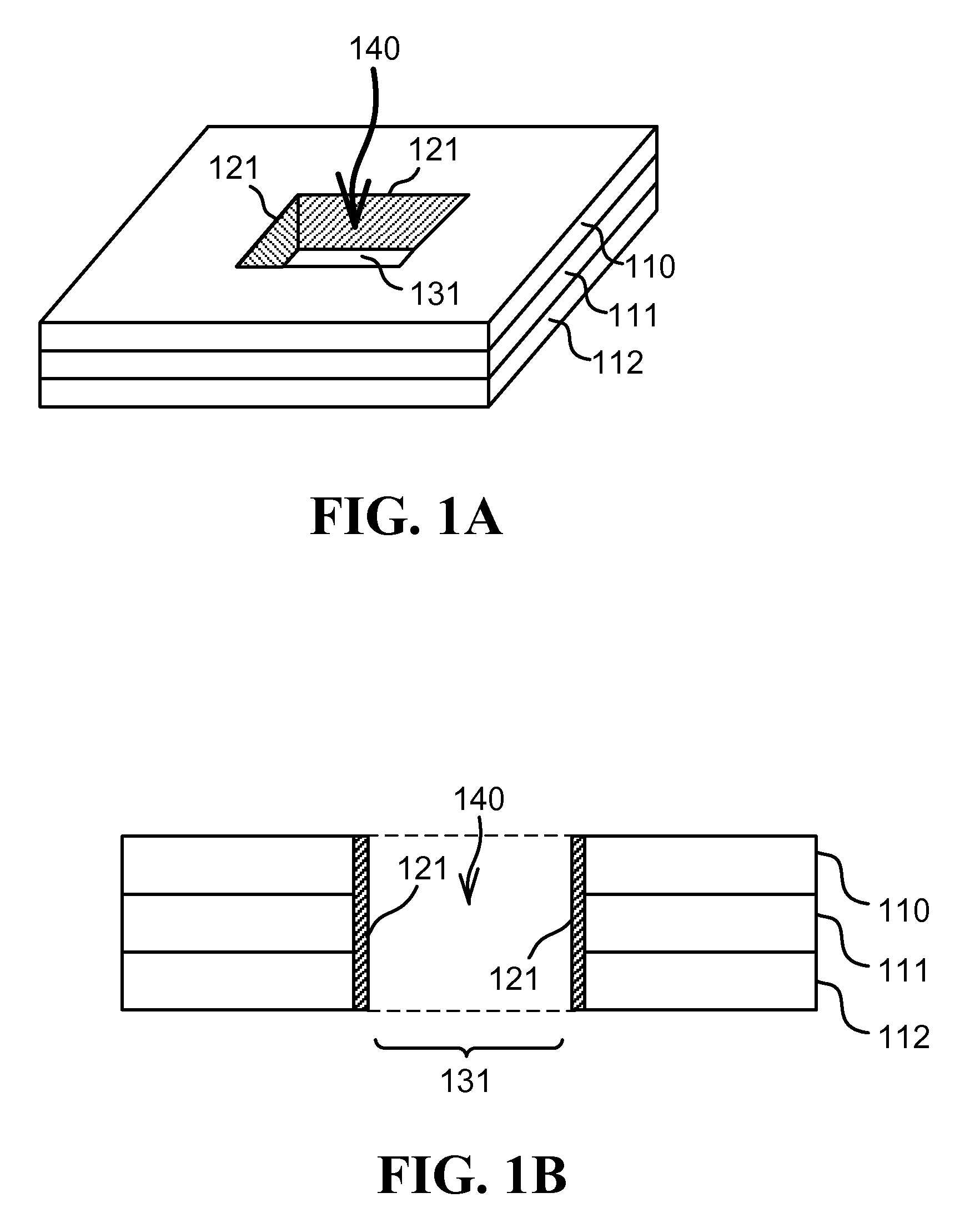
[0089]FIG. 1A and FIG. 1B illustrate one embodiment of a laminate waveguide structure configured to guide millimeter-waves through laminas. FIG. 1B is a lateral cross-section of a laminate waveguide structure illustrated by FIG. 1A. Typically such structure shall include at least two laminas. In FIG. 1A and FIG. 1B three laminas 110, 111, 112 belonging to a laminate waveguide structure are illustrated by way of example. A cavity 131 is formed perpendicularly through the laminas. An electrically conductive plating 121 is applied on the insulating walls of cavity 131...


PUM

PropertyMeasurementUnit
Frequencyaaaaaaaaaa
Electrical conductivityaaaaaaaaaa

Abstract

Various embodiments of millimeter-wave systems on a printed circuit board, including a microstrip, a probe, and an RF integrated circuit, as well as methods for manufacturing said systems. Various embodiments have holes extending through lamina in the PCB, thereby improving radiation propagation. Various embodiments have conductive cages created by multiple through-holes extending through lamina in the PCB, thereby increasing radiation propagation. The manufacture of such systems is easier and less expensive than the manufacture of current systems.

Description

TECHNICAL FIELD[0001]Some of the disclosed embodiments relate to millimeter-wave systems, and more specifically to a waveguide comprising laminate structure.BACKGROUND[0002]Some current millimeter-wave systems on a printed circuit board (“PCB”) have relatively complicated structures, with many components. Among other components, such systems may have a top layer (or “lamina”) on which a microstrip and probe are printed. Other layers (or “laminas”) in such systems may have a hole therein for better radiation propagation from the probe, but the top lamina does not have such a hole. Rather, the probe sits on the top lamina at a position above the hole that extends through the lower laminas.[0003]These current systems have several disadvantages. First, radiation propagation is degraded by the need for the radiation to propagate through the top lamina. Second, the lower layers form a waveguide structure, but the source of radiation is separated from the waveguide structure by the thickne...

Claims


Application Information

Patent Timeline
IPC IPC(8): H01P5/107H01P3/12H01P3/00H01P11/00
CPCH01P5/107H01P3/003H01P3/121H01P11/002Y10T156/1052
Inventor LEIBA, YIGALDAYAN, ELAD
Owner SIKLU COMM
Why Eureka
Try Eureka