Plasma thermal shield for heat dissipation in plasma chamber

a plasma chamber and thermal shield technology, applied in the field of semiconductor device, can solve the problems of chip and gouge formation along the severed crack formation and propagation from the edges of the die, and inability to operate the integrated circuit, etc., and achieve the effect of dissipating hea

Active Publication Date: 2016-03-22
APPLIED MATERIALS INC
View PDF100 Cites 2 Cited by
  • Summary
  • Abstract
  • Description
  • Claims
  • Application Information

AI Technical Summary

Benefits of technology

[0011]In another embodiment, a method of dicing a semiconductor wafer having a plurality of integrated circuits involves introducing a substrate supported by a substrate carrier into a plasma etch chamber. The substrate has a patterned mask thereon covering integrated circuits and exposing streets of the substrate. The method also involves clamping the substrate carrier below a shadow ring having a plasma thermal shield disposed thereon. The method also involves plasma etching the substrate through the streets to singulate the integrated circuits. The shadow ring and plasma thermal shield protect the substrate carrier from the plasma etching. The plasma thermal shield dissipates heat away from the shadow ring during the plasma etching.

Problems solved by technology

One problem with either scribing or sawing is that chips and gouges can form along the severed edges of the dies.
In addition, cracks can form and propagate from the edges of the dies into the substrate and render the integrated circuit inoperative.
Chipping and cracking are particularly a problem with scribing because only one side of a square or rectangular die can be scribed in the direction of the crystalline structure.
Consequently, cleaving of the other side of the die results in a jagged separation line.
As a result of the spacing requirements, not as many dies can be formed on a standard sized wafer and wafer real estate that could otherwise be used for circuitry is wasted.
Furthermore, after cutting, each die requires substantial cleaning to remove particles and other contaminants that result from the sawing process.
Plasma dicing has also been used, but may have limitations as well.
For example, one limitation hampering implementation of plasma dicing may be cost.
A standard lithography operation for patterning resist may render implementation cost prohibitive.
Another limitation possibly hampering implementation of plasma dicing is that plasma processing of commonly encountered metals (e.g., copper) in dicing along streets can create production issues or throughput limits.

Method used


Image

  • Plasma thermal shield for heat dissipation in plasma chamber
  • Plasma thermal shield for heat dissipation in plasma chamber
  • Plasma thermal shield for heat dissipation in plasma chamber

Examples


Embodiment Construction

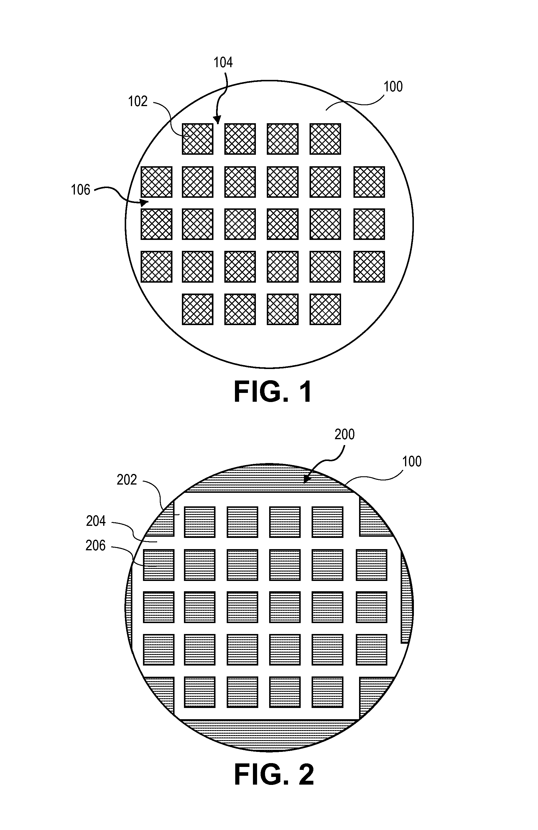
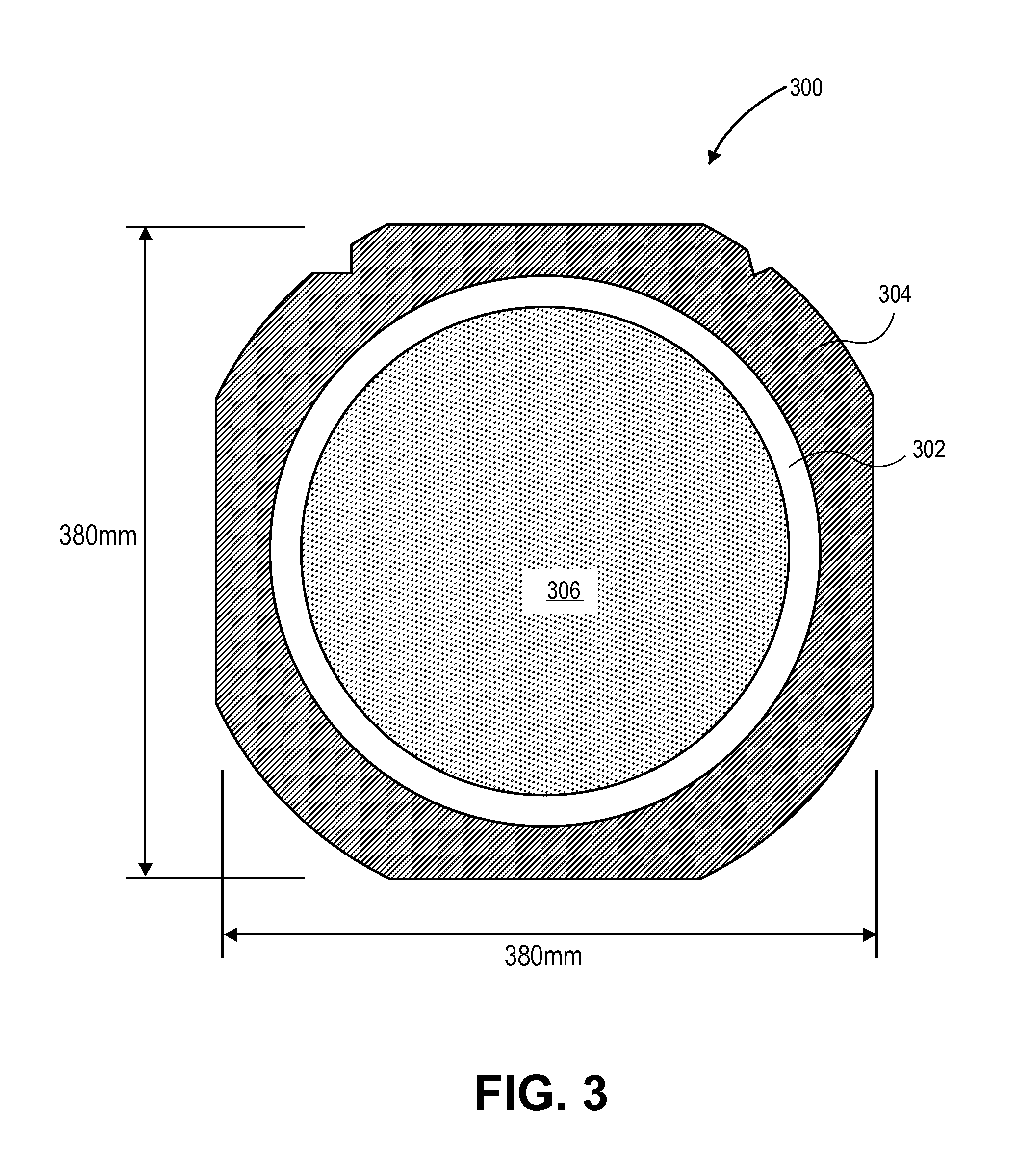
[0031]Methods of and apparatuses for dicing semiconductor wafers, each wafer having a plurality of integrated circuits thereon, are described. In the following description, numerous specific details are set forth, such as substrate carriers for thin wafers, scribing and plasma etching conditions and material regimes, in order to provide a thorough understanding of embodiments of the present invention. It will be apparent to one skilled in the art that embodiments of the present invention may be practiced without these specific details. In other instances, well-known aspects, such as integrated circuit fabrication, are not described in detail in order to not unnecessarily obscure embodiments of the present invention. Furthermore, it is to be understood that the various embodiments shown in the Figures are illustrative representations and are not necessarily drawn to scale.

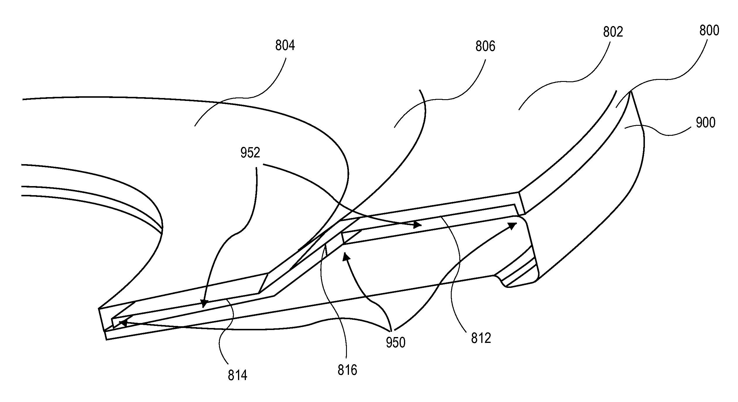
[0032]One or more embodiments described herein are directed to an actively-cooled shadow ring for heat dissipatio...


PUM


Abstract

Methods of and apparatuses for dicing semiconductor wafers, each wafer having a plurality of integrated circuits, are described. In an example, a plasma thermal shield for a plasma processing chamber includes an annular ring body having an inner opening. A plasma-facing surface of the annular ring body has a general topography. A bottom surface of the annular ring body reciprocates the general topography with recessed regions disposed therein, providing one or more protruding regions at the bottom surface of the annular ring body.

Description

BACKGROUND[0001]1) Field[0002]Embodiments of the present invention pertain to the field of semiconductor processing and, in particular, to methods of dicing semiconductor wafers, each wafer having a plurality of integrated circuits thereon.[0003]2) Description of Related Art[0004]In semiconductor wafer processing, integrated circuits are formed on a wafer (also referred to as a substrate) composed of silicon or other semiconductor material. In general, layers of various materials which are either semiconducting, conducting or insulating are utilized to form the integrated circuits. These materials are doped, deposited and etched using various well-known processes to form integrated circuits. Each wafer is processed to form a large number of individual regions containing integrated circuits known as dies.[0005]Following the integrated circuit formation process, the wafer is “diced” to separate the individual die from one another for packaging or for use in an unpackaged form within l...

Claims


Application Information

Patent Timeline
Patent Type & Authority Patents(United States)
IPC IPC(8): H01L21/00H01J37/32H01L21/78H01L21/683
CPCH01J37/32798H01J37/32477H01J37/32522H01J37/32642H01L21/6836H01L21/78H01L2221/68327H01L2221/68377
Inventor OUYE, ALAN, HIROSHI
Owner APPLIED MATERIALS INC
Why Eureka
Try Eureka