Integrating active matrix inorganic light emitting diodes for display devices

a technology of inorganic light-emitting diodes and active matrix, which is applied in the direction of basic electric elements, semiconductor devices, electrical equipment, etc., can solve the problem of not supporting the resolution needed in the next-generation display

Inactive Publication Date: 2016-03-22
GLOBALFOUNDRIES INC
View PDF22 Cites 17 Cited by
  • Summary
  • Abstract
  • Description
  • Claims
  • Application Information

AI Technical Summary

Benefits of technology

[0005]In contrast to the more established inorganic LEDs, the low deposition temperature of organic materials is well compatible with low-cost

Problems solved by technology

Despite the OLED's demonstrated superiority over the LCD, there still remain several challenging issues related to encapsulation and lifetime, yield, color efficiency, and drive electronics, all of which are receiving considerable attention.
Although

Method used


Image

  • Integrating active matrix inorganic light emitting diodes for display devices
  • Integrating active matrix inorganic light emitting diodes for display devices
  • Integrating active matrix inorganic light emitting diodes for display devices

Examples


Embodiment Construction

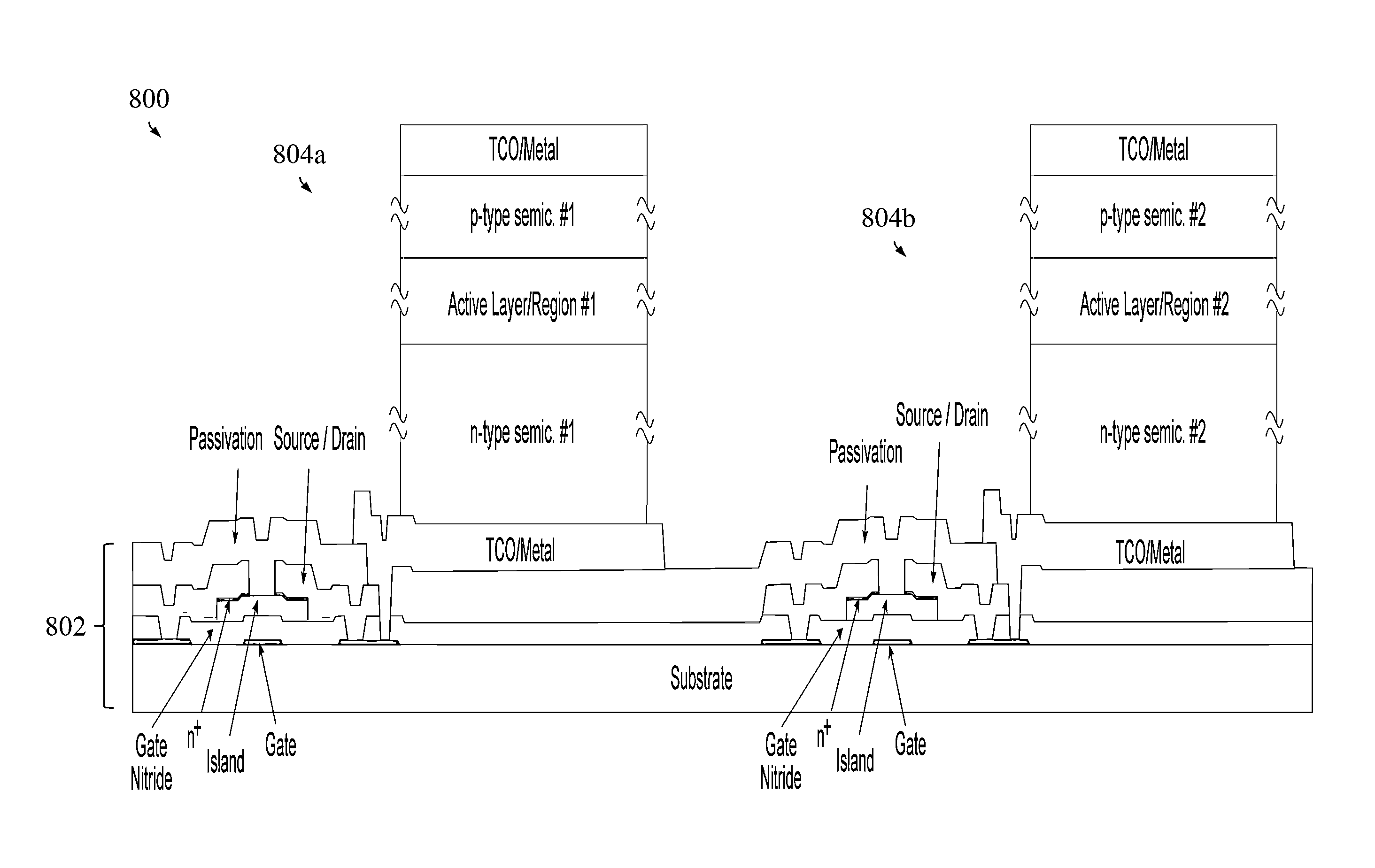
[0021]Disclosed herein is a method of integrating inorganic light emitting diodes (LEDs) onto a thin-film transistor (TFT) backplane for realizing active matrix LED displays on substrates, whether flexible or rigid substrates. In brief, the embodiments herein utilize a stress-induced, substrate spalling technique to transfer a layer of a conventionally grown, inorganic LED device onto an integrated TFT backplane using a mechanical bonding technique (such as cold welding, for example) to create an active matrix, inorganic LED array. Previously, any practical approach to integrating LED devices with TFT backplane substrates was through the low temperature deposition of the aforementioned organic LED material.

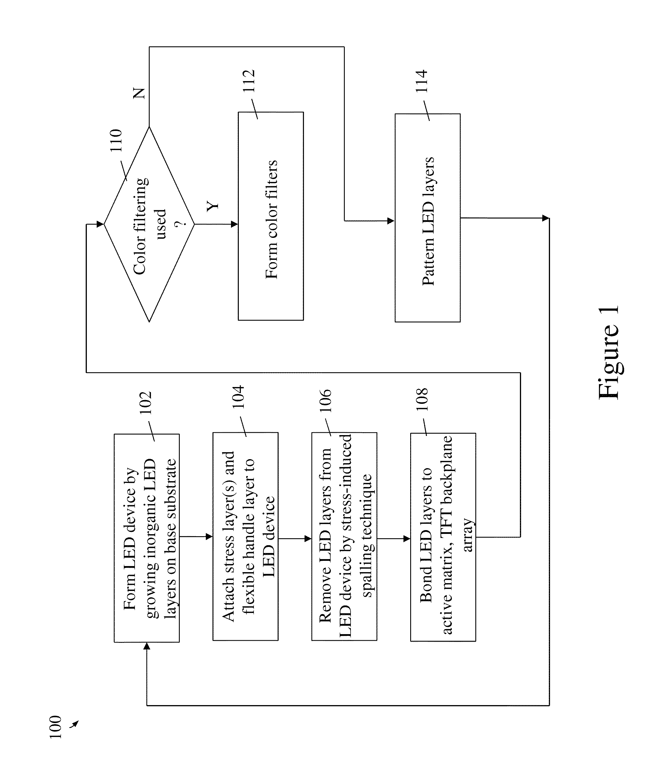
[0022]Referring initially to FIG. 1, there is shown a flow diagram illustrating a method 100 of forming an active matrix, inorganic LED array in accordance with an exemplary embodiment. FIG. 1 may be referenced again later as specific operations depicted in the flow diagram blocks...


PUM


Abstract

A method of forming an active matrix, light emitting diode (LED) array includes removing, from a base substrate, a layer of inorganic LED material originally grown thereupon; and bonding the removed layer of inorganic LED material to an active matrix, thin film transistor (TFT) backplane array.

Description

DOMESTIC PRIORITY[0001]This application is a divisional of U.S. patent application Ser. No. 13 / 303,486, filed Nov. 23, 2011, the disclosure of which is incorporated by reference herein in its entirety.BACKGROUND[0002]The present invention relates generally to semiconductor device manufacturing and, more particularly, to methods of integrating active matrix, inorganic light emitting diodes for display devices.[0003]Organic light emitting diode (OLED) displays have gained significant interest recently in flat panel display applications in view of their faster response times, larger viewing angles, higher contrast, lighter weight, lower power, amenability to flexible substrates, as compared to liquid crystal displays (LCDs). Despite the OLED's demonstrated superiority over the LCD, there still remain several challenging issues related to encapsulation and lifetime, yield, color efficiency, and drive electronics, all of which are receiving considerable attention.[0004]Nonetheless, OLEDs...

Claims


Application Information

Patent Timeline
IPC IPC(8): H01L27/12H01L27/15H01L33/00
CPCH01L33/42H01L27/156H01L33/0093H01L27/1214H01L33/62H01L27/1218
Inventor BEDELL, STEPHEN W.HEKMATSHOARTABARI, BAHMANSADANA, DEVENDRA K.SHAHIDI, GHAVAM G.SHAHRJERDI, DAVOOD
Owner GLOBALFOUNDRIES INC
Why Eureka
Try Eureka