
Nanometric imprint lithography method

a lithography method and nanotechnology, applied in the field of lithography methods, can solve the problems of nanoimprinting patterns that are difficult to remove, require considerable investment, and difficult to achieve, and achieve the effects of reducing the resistance, and reducing the cost of implementation

Active Publication Date: 2016-04-05
COMMISSARIAT A LENERGIE ATOMIQUE ET AUX ENERGIES ALTERNATIVES
View PDF12 Cites 0 Cited by
  • Summary
  • Abstract
  • Description
  • Claims
  • Application Information

AI Technical Summary

Benefits of technology

The invention allows for very precise and simple removal of resist in the bottom of patterns, eliminating the need for normally used steps of RIE or post-etching. The exposure step uses multiple light sources with different wavelengths to increase absorption.

Problems solved by technology

In particular, in order to limit the diffraction of light through the masks, it is necessary to have recourse to shorter wavelengths (ultraviolet, or even X-rays) and complex techniques (for example immersion lithography), which require considerable investments for development and industrial implementation thereof.
The insolation causes the hardening of the resist.
These known techniques of removing the residue present in the bottom of the nanoimprinted patterns are relatively complicated, lengthy and expensive to implement.

Method used


Image

  • Nanometric imprint lithography method
  • Nanometric imprint lithography method
  • Nanometric imprint lithography method

Examples


Embodiment Construction

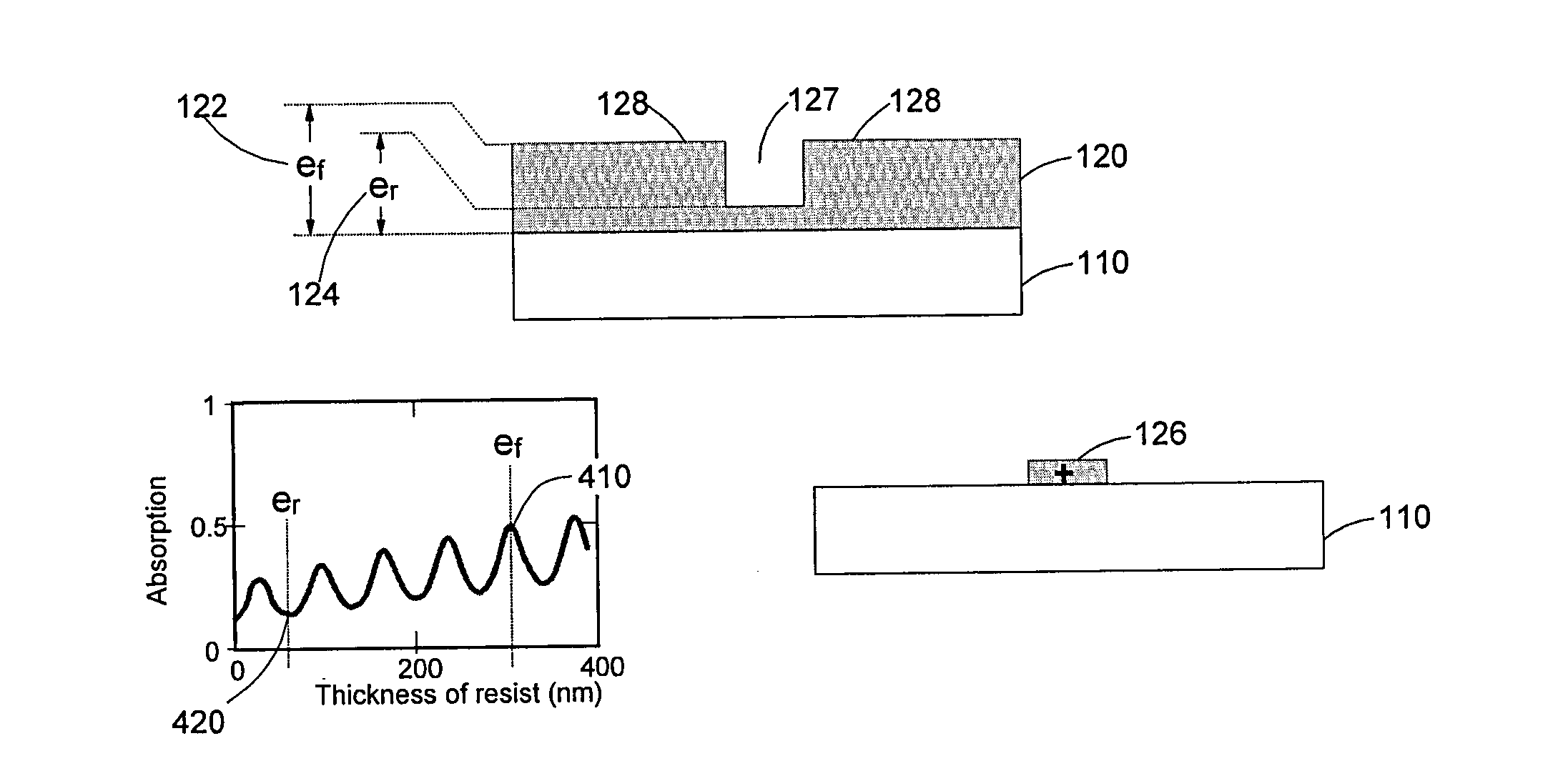
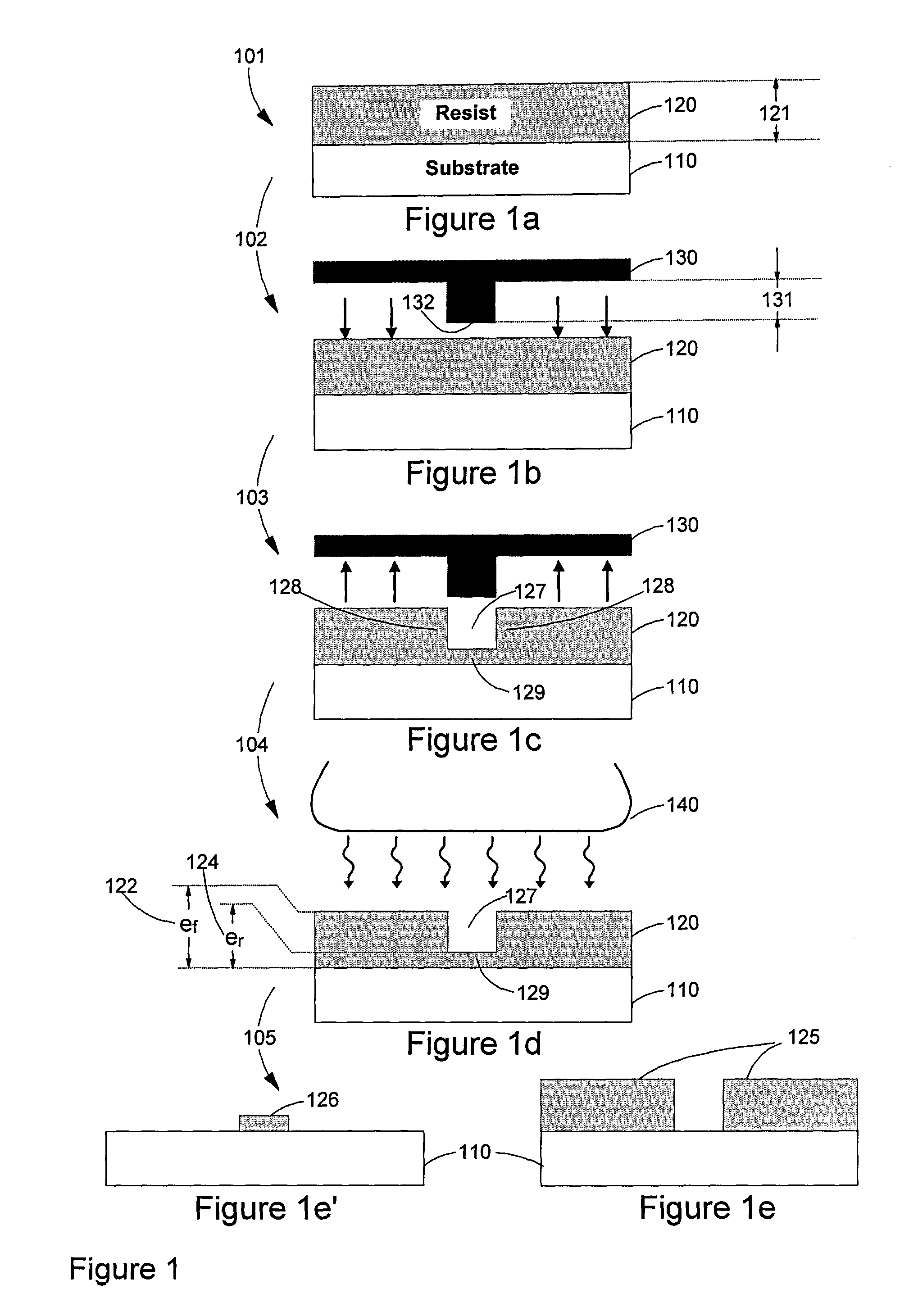
[0060]FIG. 1, which comprises FIGS. 1a to 1e′, illustrates the steps of the improved nanometric imprint lithography method of the invention.

[0061]On the substrate 110 where, on the surface, it is wished to reproduce and etch patterns that will contribute to the production of a device being manufactured, a layer of a photosensitive resist 120 is deposited, for example, of the type used in a standard manner by the microelectronics industry for optical lithography. The invention makes no assumption on the type of substrate by which the method of the invention is implemented. In particular, the substrate may for example already comprise numerous layers (not shown) on the surface, in which patterns may already have been previously defined, with the method of the invention, or by other means in particular using conventional optical lithography or electronic lithography.

[0062]As shown in FIG. 1a, the first step 101 therefore consists of depositing on the surface a layer of resist preferabl...


PUM

PropertyMeasurementUnit
wavelengthaaaaaaaaaa
thicknessaaaaaaaaaa
thicknessesaaaaaaaaaa

Abstract

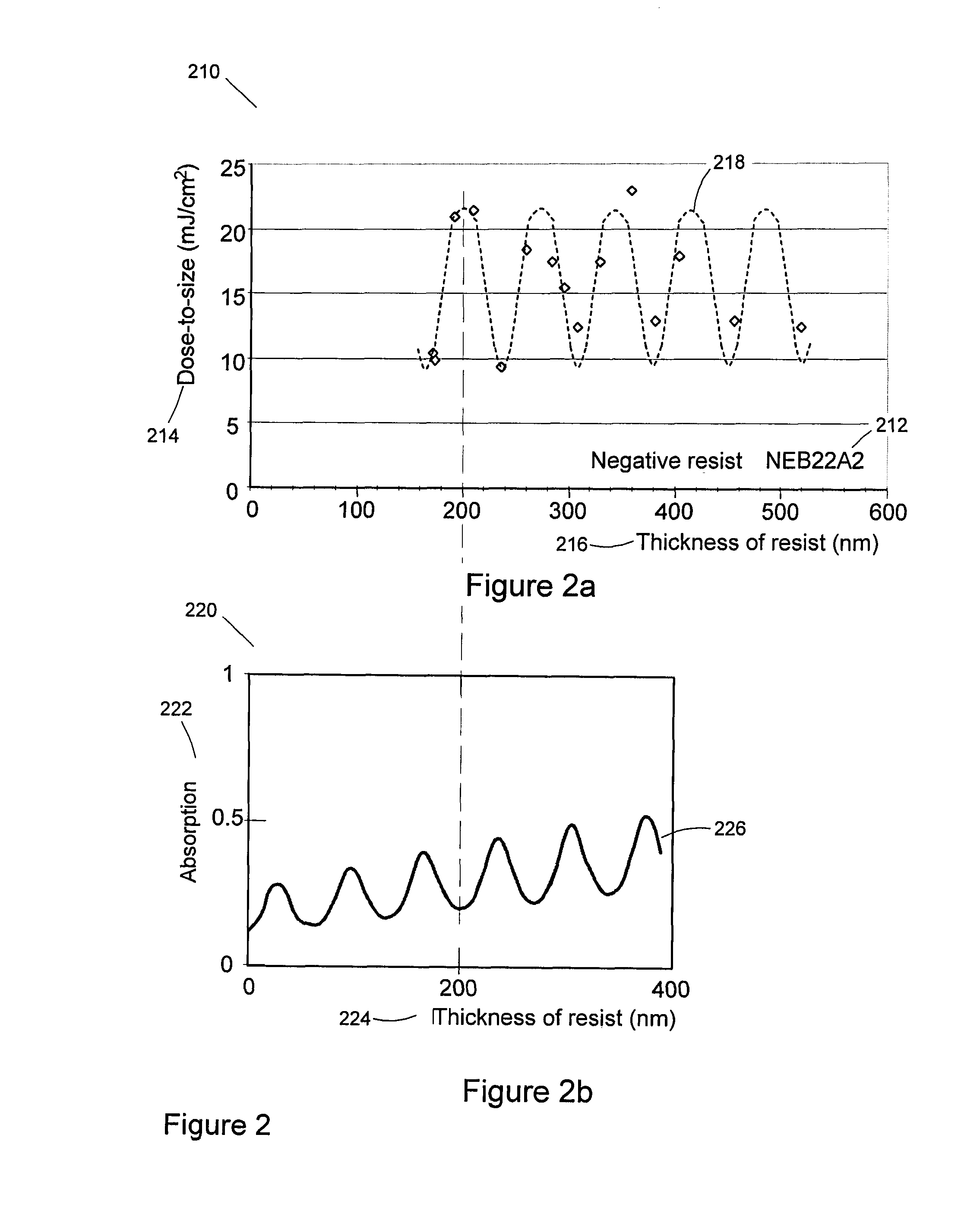
A nanoimprint lithography method, including: pressing a mold in a photosensitive resin to form at least one imprint pattern defined by a stamped area and an adjacent area, the adjacent area being less stamped or not stamped at all, and being thicker than the stamped area; and exposure to a certain amount of sunlight. Respective thicknesses of the two areas are defined such that the two areas absorb a different amount of the sunlight and the amount of sunlight provided by the exposure is predetermined so as to be great enough to activate the resin in whichever of the two areas has the greater absorption, and so as not to be great enough to activate the other of the two areas.

Description

TECHNICAL FIELD OF THE INVENTION[0001]The present invention concerns in general lithography methods. It receives as a favoured application the lithography methods used by the microelectronics industry for manufacturing semiconductor devices, in particular integrated circuits. It concerns more particularly an improved nanometric imprint lithography method.PRIOR ART[0002]The industrial manufacture of new generations of integrated circuits involves being able to etch patterns of ever smaller sizes, which are now measured in nanometers (nm=10−9 meters) only. The photolithography used from the start, based on the insolation of photosensitive resists through optical masks reproducing the patterns to be etched, does however come up against physical barriers which require having recourse to more and more sophisticated techniques in order to be able to accompany the growth of the required integration density. In particular, in order to limit the diffraction of light through the masks, it is ...

Claims


Application Information

Patent Timeline
Patent Type & Authority Patents(United States)
IPC IPC(8): G03F7/00B82Y40/00H01L21/033B82Y10/00
CPCH01L21/0337B82Y10/00B82Y40/00G03F7/0002Y10S977/887Y10T428/24612
Inventor PAULIAC, SEBASTIEN
Owner COMMISSARIAT A LENERGIE ATOMIQUE ET AUX ENERGIES ALTERNATIVES
Learn More