Light emitting device, method for manufacturing light emitting device, and package array

a technology for light emitting devices and manufacturing methods, applied in semiconductor/solid-state device manufacturing, semiconductor devices, electrical devices, etc., can solve the problems of reducing the manufacturing yield poor standing stability, and difficulty in increasing the number of lead pieces that can be punched out from a single piece of sheet metal, so as to reduce the inclination of light emitting devices during mounting and reduce the effect of the manufacturing yield

Active Publication Date: 2016-04-12
NICHIA CORP
View PDF34 Cites 0 Cited by
  • Summary
  • Abstract
  • Description
  • Claims
  • Application Information

AI Technical Summary

Benefits of technology

[0008]However, when a plurality of lead pieces are punched out from a single piece of sheet metal, since each of the leads has wing parts, it is difficult to increase the number of lead pieces that can be punched out from a single piece of sheet metal. This is a problem because it decreases the manufacturing yield of the light emitting device.
[0009]The present invention was conceived in light of the above situation, and it is an object thereof to provide a light emitting device, a method for manufacturing a light emitting device, and a package array with which the decrease in the manufacturing yield can be reduced.
[0011]Therefore, the first convex part is formed by stamping form the rear face side, which is obvious since the first concave part is formed. Accordingly, the number of lead pieces that can be punched out from a single lead frame can be increased, so there is less of a decrease in the manufacturing yield of the light emitting device.
[0014]In view of this, with the light emitting device pertaining to the second aspect, since the terminal part is exposed from the lower face to the side face of the package, during mounting the molten solder is allowed to creep up from the lower face to the side face of the package, so the stress produced by the surface tension of the solder is also exerted in the side face direction. This reduces inclination of the light emitting device during mounting.
[0015]The present invention provides a light emitting device, a method for manufacturing a light emitting device, and a package array with which the decrease in the manufacturing yield can be reduced.

Problems solved by technology

However, when a plurality of lead pieces are punched out from a single piece of sheet metal, since each of the leads has wing parts, it is difficult to increase the number of lead pieces that can be punched out from a single piece of sheet metal.
This is a problem because it decreases the manufacturing yield of the light emitting device.
A problem here is that with a side-view type of light emitting device, the standing stability is poor because of the low ratio of depth to height.

Method used


Image

  • Light emitting device, method for manufacturing light emitting device, and package array
  • Light emitting device, method for manufacturing light emitting device, and package array
  • Light emitting device, method for manufacturing light emitting device, and package array

Examples


Embodiment Construction

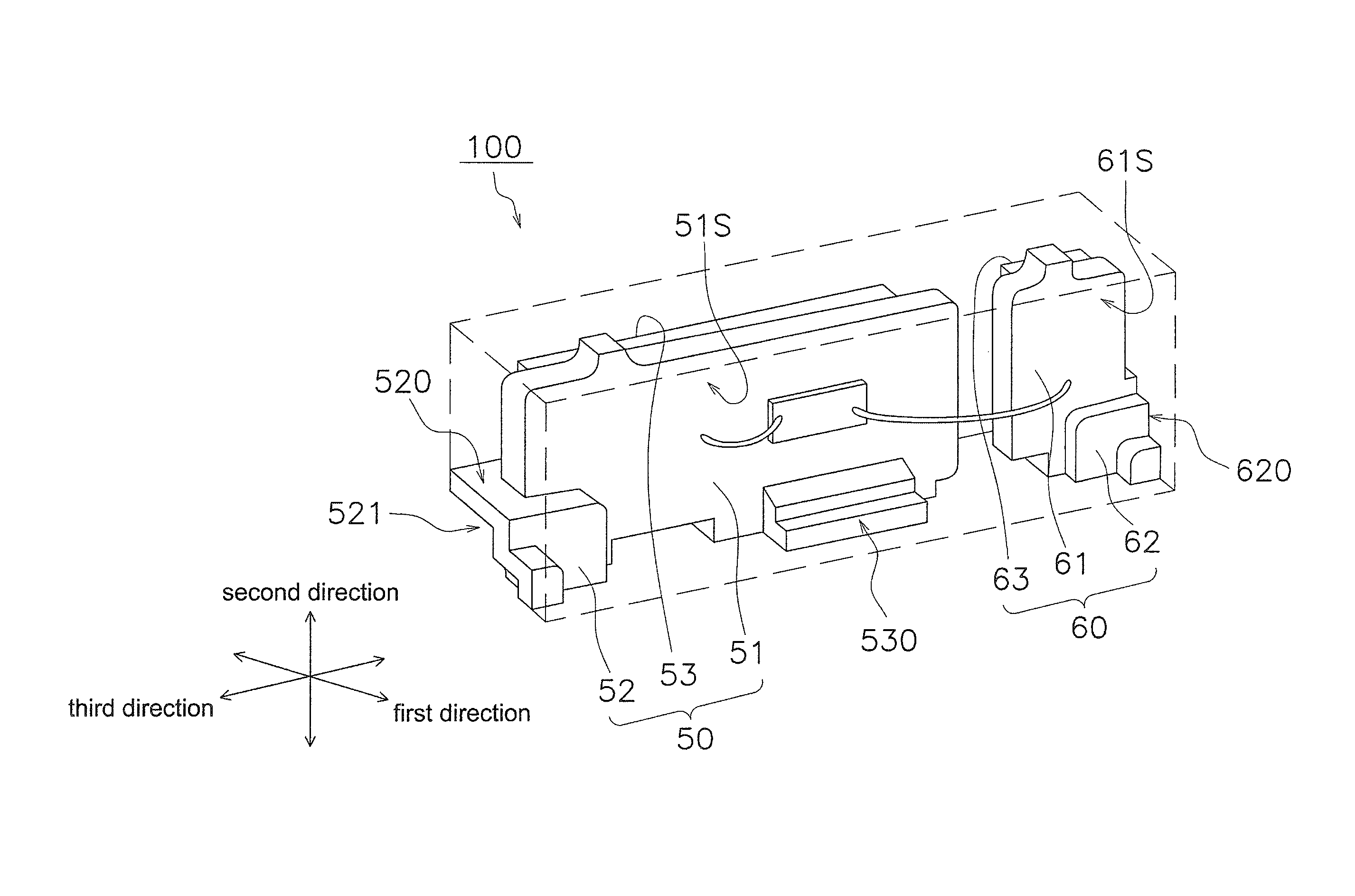
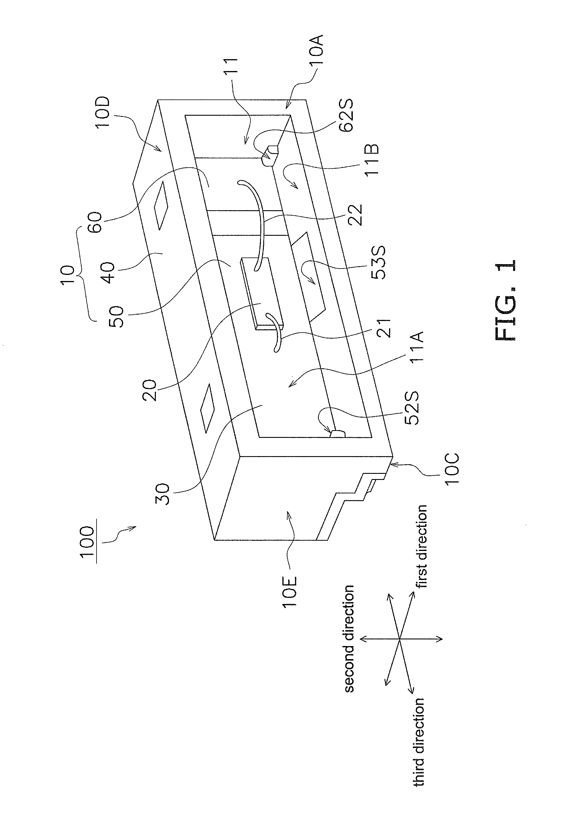
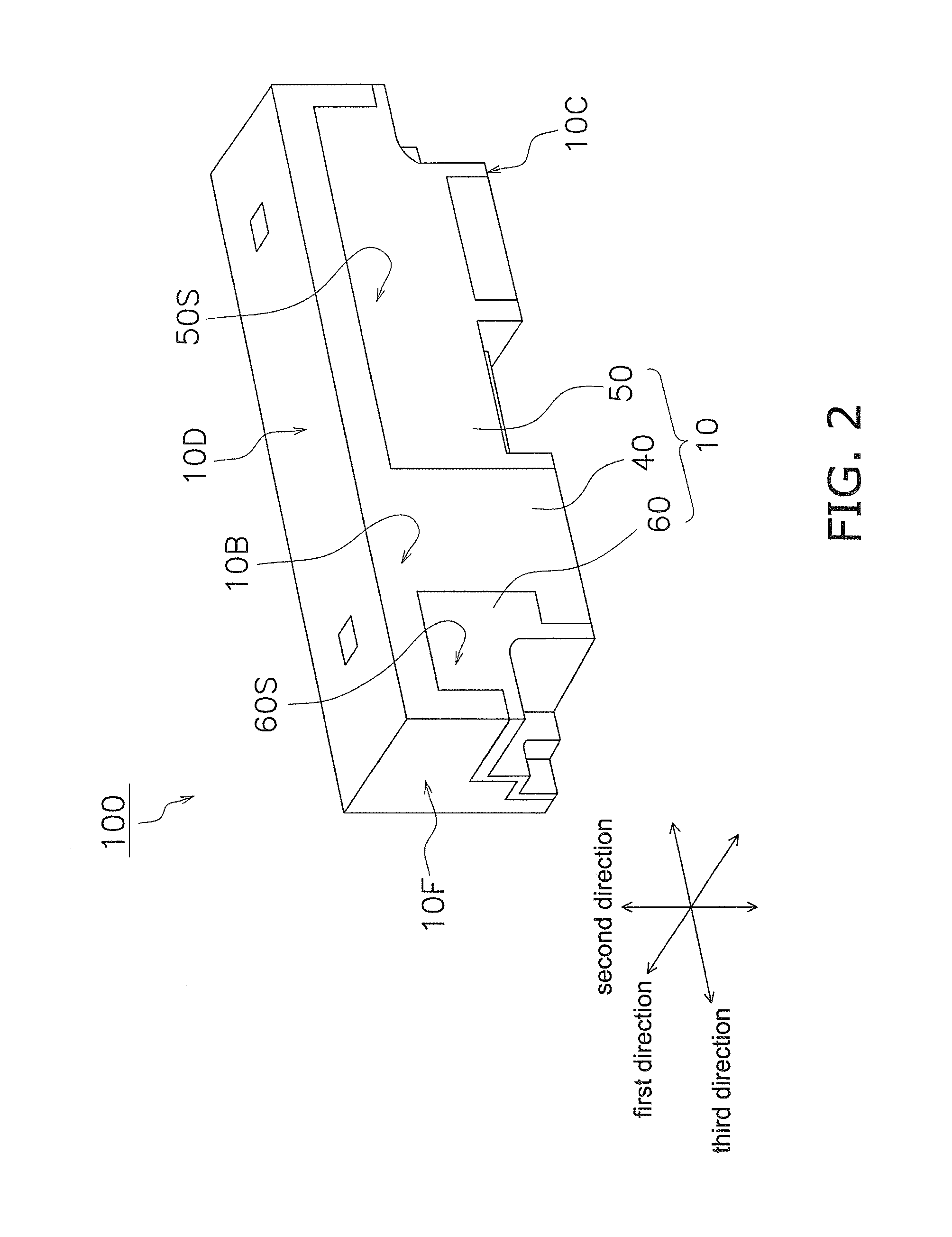
[0034]Embodiments of the present invention will now be described through reference to the drawings. In the following description of the drawings, those portions that are the same or similar will be numbered the same or similarly. The drawings, however, are merely schematics, and the various dimensional ratios and so forth may be different from those in actuality. Therefore, specific dimensions and the like should be determined by consulting the following description. Naturally, there may be situations in which the dimensional relations and ratios vary from one drawing to the next.

[0035]In the following embodiment, a side view type of light emitting device will be described as an example of a light emitting device. A side view type of light emitting device is a type in which light emitted by the light emitting element is taken off in a direction parallel to the mounting face of the mounting board. However, the technology disclosed herein can also be applied to a top view type of ligh...


PUM


Abstract

In a light emitting device, a first lead has a first terminal part that is contiguous with a first connector. The first terminal part includes a first convex part that is exposed from a molded article at the inner peripheral face of a mounting recess, and a first concave part that is formed in the rear face of the first convex part.

Description

CROSS-REFERENCE TO RELATED APPLICATIONS[0001]This application claims priority to Japanese Patent Application Nos. 2011-027214 and 2011-027209 both filed on Feb. 10, 2011. The entire disclosures of Japanese Patent Application Nos. 2011-027214 and 2011-027209 are hereby incorporated herein by reference.BACKGROUND OF THE INVENTION[0002]1. Field of the Invention[0003]The present invention relates to a light emitting device comprising a light emitting element, to a method for manufacturing a light emitting device, and to a package array.[0004]2. Background Art[0005]Light emitting devices equipped with a light emitting element (such as a light emitting diode or a laser diode) have been widely used in the past as light sources for optical communications devices, lighting fixtures, liquid crystal television backlights, and so forth.[0006]In a light emitting device such as this, the light emitting element is disposed in a mounting recess of a package including leads and a molded article. The...

Claims


Application Information

Patent Timeline
Patent Type & Authority Patents(United States)
IPC IPC(8): H01L33/62H01L33/48
CPCH01L33/62H01L33/486H01L2224/48091H01L2224/48247H01L2224/48257H01L2933/0033H01L2924/00014H01L33/60
Inventor YAMASHITA, RYOHEI
Owner NICHIA CORP
Why Eureka
Try Eureka