Methods of manufacturing electronic devices formed in a cavity

a manufacturing method and cavity technology, applied in the direction of manufacturing tools, non-electric welding apparatus, welding apparatus, etc., can solve the problems of unnecessarily extending cycle time, reducing manufacturing yield, and lowering manufacturing yield, so as to reduce cycle time and reduce manufacturing yield. , the effect of lowering the manufacturing yield

Active Publication Date: 2018-06-07
SKYWORKS SOLUTIONS INC
View PDF0 Cites 0 Cited by
  • Summary
  • Abstract
  • Description
  • Claims
  • Application Information

AI Technical Summary

Benefits of technology

[0005]Some conventional methods of fabricating electronic devices include gold-gold bonding or copper-copper bonding that require a high temperature and pressure process that may cause the device substrate, the cap substrate, and the like to be damaged and the manufacturing yield to be lowered. These conventional processes may include repeated cycles between a normal temperature and pressure step and a high temperature and pressure step, which may cause the cycle time to be unnecessarily elongated. Still further, in these conventional processes defects may occur due to overetching in a process of forming a through-hole, lowering the manufacturing yield.
[0006]Aspects of the present disclosure provide an electronic device and a method of manufacturing the electronic device that may be used to improve the yield, shorten the cycle time, prevent defects occurring due to overetching in a process of forming a through-hole, or all of the above.

Problems solved by technology

Some conventional methods of fabricating electronic devices include gold-gold bonding or copper-copper bonding that require a high temperature and pressure process that may cause the device substrate, the cap substrate, and the like to be damaged and the manufacturing yield to be lowered.
These conventional processes may include repeated cycles between a normal temperature and pressure step and a high temperature and pressure step, which may cause the cycle time to be unnecessarily elongated.
Still further, in these conventional processes defects may occur due to overetching in a process of forming a through-hole, lowering the manufacturing yield.

Method used


Image

  • Methods of manufacturing electronic devices formed in a cavity
  • Methods of manufacturing electronic devices formed in a cavity
  • Methods of manufacturing electronic devices formed in a cavity

Examples


Embodiment Construction

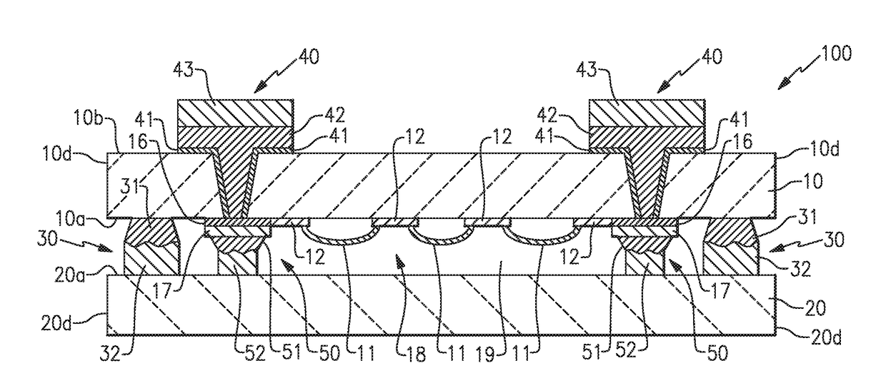
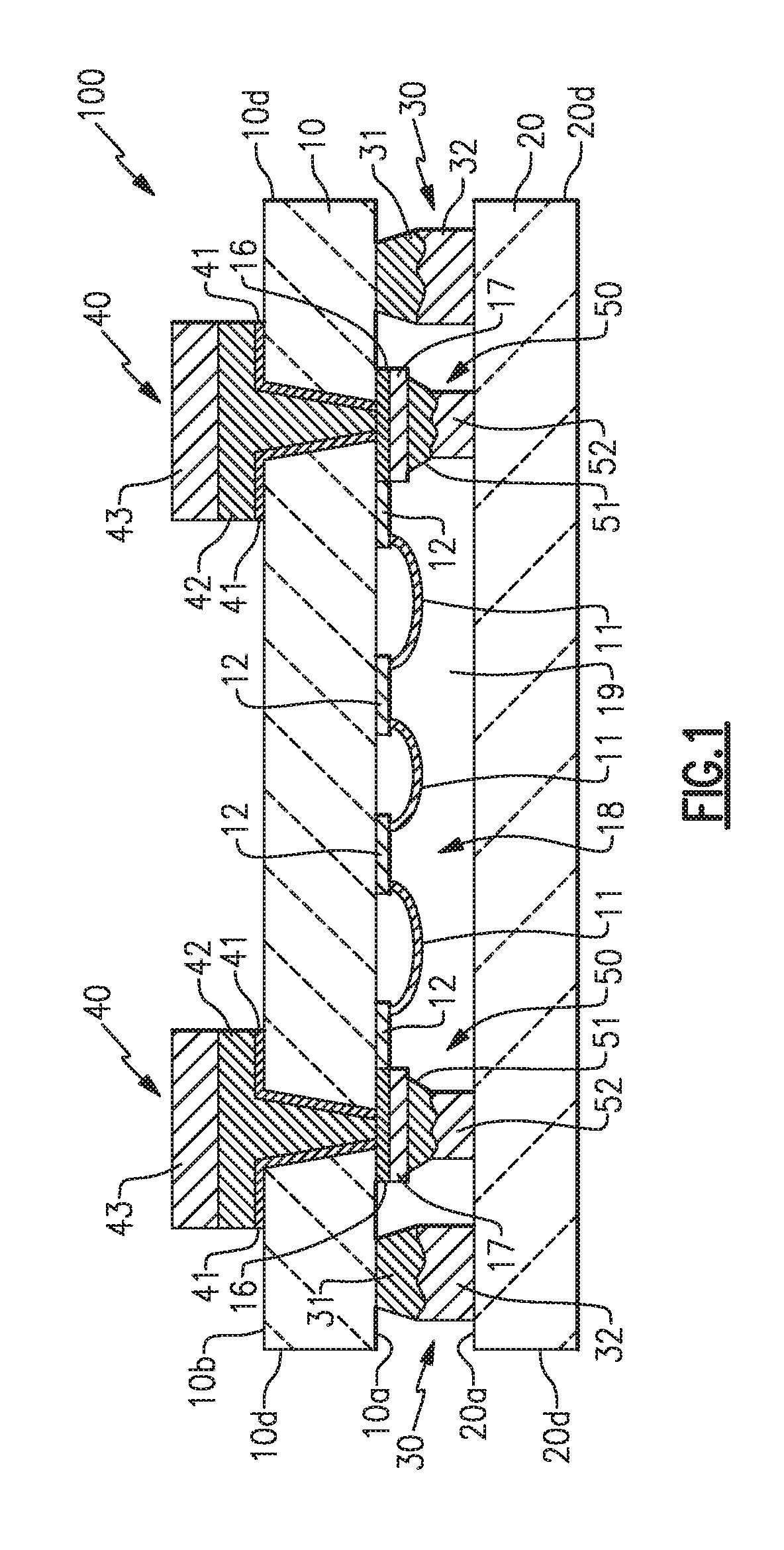
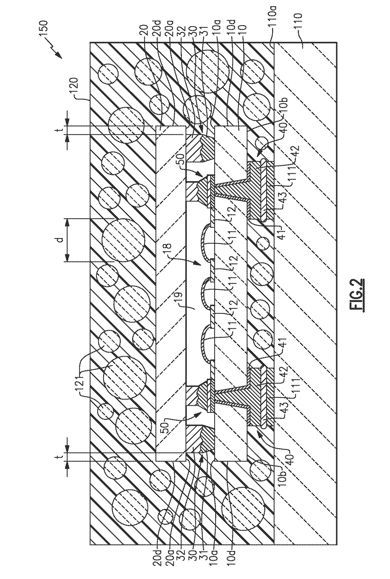
[0059]It is to be appreciated that embodiments of the methods and apparatuses discussed herein are not limited in application to the details of construction and the arrangement of components set forth in the following description or illustrated in the accompanying drawings. The methods and apparatuses are capable of implementation in other embodiments and of being practiced or of being carried out in various ways. Examples of specific implementations are provided herein for illustrative purposes only and are not intended to be limiting. Also, the phraseology and terminology used herein is for the purpose of description and should not be regarded as limiting. The use herein of “including,”“comprising,”“having,”“containing,”“involving,” and variations thereof is meant to encompass the items listed thereafter and equivalents thereof as well as additional items. References to “or” may be construed as inclusive so that any terms described using “or” may indicate any of a single, more tha...


PUM

PropertyMeasurementUnit
temperatureaaaaaaaaaa
temperaturesaaaaaaaaaa
temperatureaaaaaaaaaa

Abstract

Methods of manufacturing an electronic device formed in a cavity may include providing a first substrate having a first side wall including a first metal formed along a periphery on a bottom surface thereof and surrounding an electronic circuit disposed on the bottom surface, providing a second substrate having a second side wall including a second metal and a third metal formed along a periphery on a top surface thereof, aligning the first substrate with the second substrate with the first side wall opposing and contacting the second side wall to internally define a cavity between the bottom surface of the first substrate, the top surface of the second substrate, the first side wall ,and the second side wall, and heating and bonding the first substrate and the second substrate by transient liquid phase bonding.

Description

CROSS-REFERENCE TO RELATED APPLICATIONS[0001]This application claims priority under 35 U.S.C. § 119(e) to each of U.S. Provisional Patent Application Ser. No. 62 / 429,218, titled “METHODS OF MANUFACTURING ELECTRONIC DEVICES FORMED IN A CAVITY HAVING REDUCED INSERTION LOSS,” filed Dec. 2, 2016, U.S. Provisional Patent Application Ser. No. 62 / 429,223, titled “METHODS OF MANUFACTURING ELECTRONIC DEVICES TO PREVENT WATER INGRESS DURING MANUFACTURE,” filed Dec. 2, 2016, U.S. Provisional Patent Application Ser. No. 62 / 539,863, titled “METHODS OF MANUFACTURING ELECTRONIC DEVICES TO PREVENT WATER INGRESS DURING MANUFACTURE,” filed Aug. 1, 2017, U.S. Provisional Patent Application Ser. No. 62 / 429,226, titled “METHODS OF MANUFACTURING ELECTRONIC DEVICES TO PREVENT DAMAGE DURING DICING,” filed Dec. 2, 2016, U.S. Provisional Patent Application Ser. No. 62 / 429,179, titled “METHODS OF MANUFACTURING ELECTRONIC DEVICES FORMED IN A CAVITY,” filed Dec. 2, 2016, U.S. Provisional Patent Application Ser....

Claims


Application Information

Patent Timeline
Patent Type & Authority Applications(United States)
IPC IPC(8): H03H3/02B23K20/16
CPCH03H3/02B23K20/16H03H2003/021B23K2201/36B23K1/0016B23K26/402B23K26/382B23K2101/42B23K2103/172H03H9/1035H03H9/0523H01L21/187H01L2224/13025H01L2924/181H01L24/16H01L24/13H01L2924/16235H01L2224/16145H01L24/81H01L2224/13082H01L24/94H01L2224/16225H01L2224/1403H01L24/14H01L24/05H01L2224/0401H01L21/6836H01L2221/68327H01L2221/6834H01L2224/13147H01L2224/05147H01L2224/05171H01L2224/05644H01L2224/056H01L2224/80399H01L2224/13109H01L2224/05166H01L2224/13144H01L2224/13111H01L2924/00012H01L2924/00014H01L2924/014H03H9/171H01L2224/83825H01L24/83H03H9/706H01L2224/83096H01L2224/8312B23K2101/36H10N30/073H10N30/086H10N30/088H01L2924/01029H01L2924/01049H01L2924/0105H01L2924/01079H03H9/17H01L25/0657H03H9/173H03H9/175
Inventor TAKANO, ATSUSHI
Owner SKYWORKS SOLUTIONS INC
Why Eureka
Try Eureka