Semiconductor device

Inactive Publication Date: 2008-05-13
RENESAS ELECTRONICS CORP
View PDF8 Cites 0 Cited by
  • Summary
  • Abstract
  • Description
  • Claims
  • Application Information

AI Technical Summary

Benefits of technology

[0004]According to the studies by the present inventors, in a glass-sealed type semiconductor device, it was found that high-temperature glass sealing causes various defects. For example, in a glass-sealed type Schottky barrier diode, a metal electrode in the Schottky barrier diode reacts to a silicon semiconductor region in glass sealing to cause a silicide layer to be formed, and a backward leakage current may be increased. This decreases a manufacturing yield of semiconductor devices and increases the manufacturing cost of the semiconductor devices. In a switching diode using a PN junction, a zener diode, or the like, high-temperature glass sealing increases compression stress or tensile stress, the reliability of an electric connection between the diode and the Dumet electrode which are sealed may be deteriorated. This decreases the manufacturing yield of semiconductor devices and increases the manufacturing cost of the semiconductor devices.
[0006]It is an object of the present invention to provide a semiconductor device the reliability of which can be improved.
[0007]It is another object of the present invention to provide a semiconductor device the manufacturing cost of which can be reduced.

Problems solved by technology

According to the studies by the present inventors, in a glass-sealed type semiconductor device, it was found that high-temperature glass sealing causes various defects.
This decreases a manufacturing yield of semiconductor devices and increases the manufacturing cost of the semiconductor devices.
In a switching diode using a PN junction, a zener diode, or the like, high-temperature glass sealing increases compression stress or tensile stress, the reliability of an electric connection between the diode and the Dumet electrode which are sealed may be deteriorated.
This decreases the manufacturing yield of semiconductor devices and increases the manufacturing cost of the semiconductor devices.
However, it was found that, when the glass sealing temperature is decreased by using a low-melting-point glass, adhesion properties between the glass and a Dumet wire serving as an internal electrode is deteriorated.
This may cause the deterioration of the reliability of the glass-sealed type semiconductor device to deteriorate the manufacturing yield and to increase the manufacturing cost of semiconductor devices.

Method used


Image

  • Semiconductor device
  • Semiconductor device
  • Semiconductor device

Examples


embodiment 1

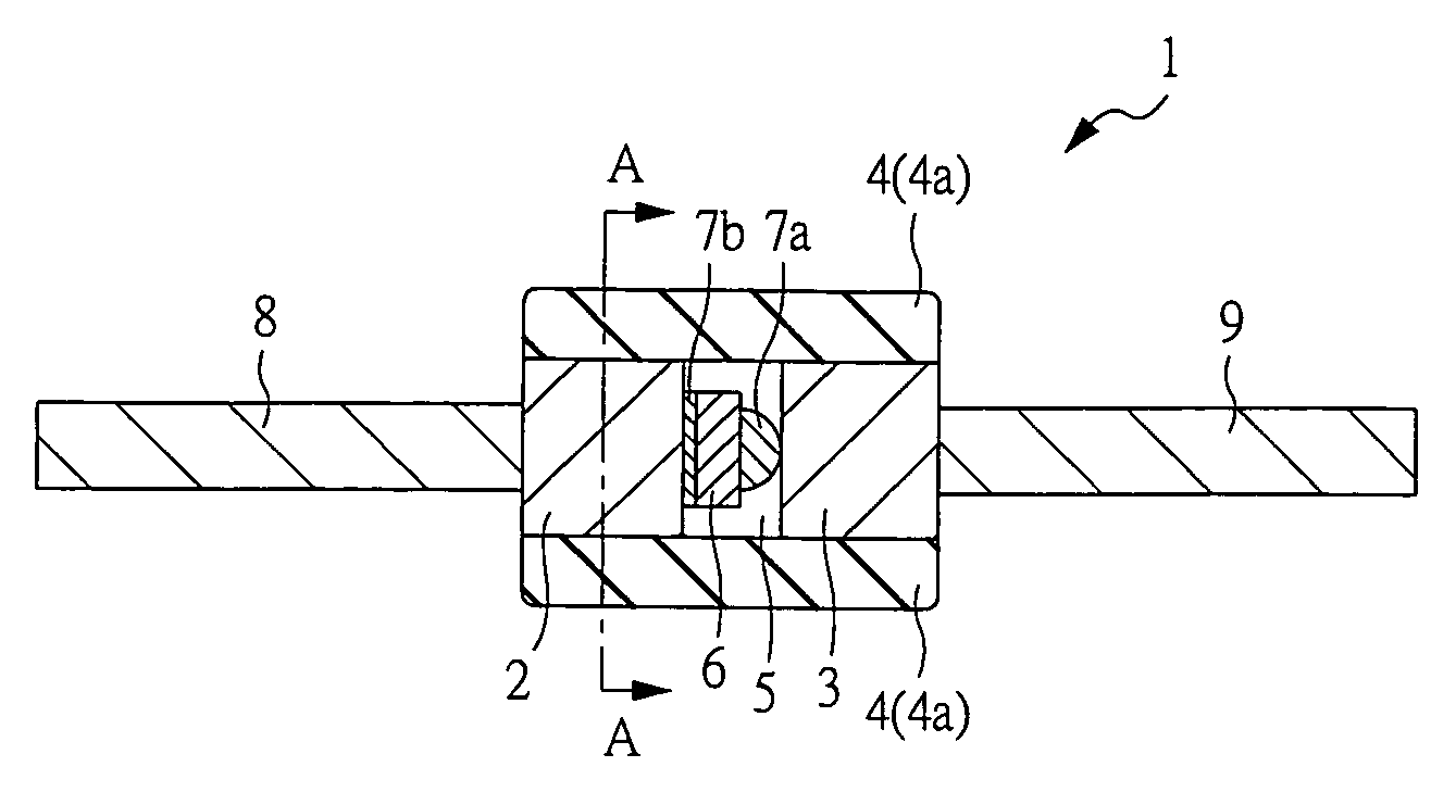
[0040]A semiconductor device according to this embodiment will be described below with reference to the drawings. FIG. 1 is a sectional view showing the structure of a semiconductor device according to an embodiment of the present invention.

[0041]A semiconductor device 1 shown in FIG. 1 is a glass-sealed type semiconductor device, for example a glass-sealed type diode. As shown in FIG. 1, the semiconductor device 1 includes electrodes constituted by Dumet wires, i.e., Dumet electrodes 2 and 3, a glass sealing member (glass tube or glass sleeve) 4, and a semiconductor element 6 (semiconductor chip) airtightly sealed (enclosed or airproof sealed) in a cavity 5 constituted by the Dumet electrodes 2 and 3 and the glass sealing member 4.

[0042]The glass sealing member 4 has a tubular (cylindrical) shape. The Dumet electrode 2 and the Dumet electrode 3 are arranged to face each other through the semiconductor element 6. The Dumet electrodes 2 and 3 and the semiconductor element 6 interpose...

second embodiment

[0087]In the first embodiment, a Schottky barrier diode is used as the semiconductor element 6 glass-sealed in the semiconductor device 1. In the second embodiment, a diode element except for a Schottky barrier diode, e.g., a semiconductor element (semiconductor chip) constituted by a diode element using a PN junction is used in place of the semiconductor element 6.

[0088]FIGS. 15 to 18 are main sectional views of steps in manufacturing a semiconductor element (semiconductor chip) 6a used in the semiconductor device according to the embodiment.

[0089]As shown in FIG. 15, a semiconductor substrate semiconductor wafer) 51 comprised of n+-type silicon in which an impurity (for example, arsenic (As) or phosphor (P)) having an n-type conductivity is doped at a high concentration is prepared. An epitaxial layer (epitaxial silicon layer) 52 having an n−-type conductivity is formed on the semiconductor substrate 51 by using a vapor-phase growth (epitaxial growth). An impurity (for example, ar...

third embodiment

[0101]In the first and second embodiments, diodes are used as the semiconductor elements 6 glass-sealed in the semiconductor device 1. In this embodiment, a semiconductor element (semiconductor chip) except for the diode is used in place of the semiconductor element 6.

[0102]FIG. 20 is a sectional view of a semiconductor device 1baccording to the embodiment, and corresponds to FIG. 1.

[0103]As shown in FIG. 20, the semiconductor device 1b of the embodiment is a glass-sealed type semiconductor device, and can function as a non-contact type electronic tag having, e.g., a microwave receiving antenna. In the semiconductor device 1b, a semiconductor element (semiconductor chip) 6b is airtightly sealed (enclosed) in a cavity 5 constituted by Dumet electrodes 2 and 3 and a glass sealing member (glass tube or glass sleeve) 4. External leads 8 and 9 are connected to the Dumet electrodes 2 and 3, respectively. The semiconductor device 1b has almost the same configuration as that of the semicond...


PUM


Abstract

A glass-sealed type semiconductor device has Dumet electrodes, a glass sealing member, and a semiconductor element tightly sealed in a cavity constituted by the Dumet electrodes and the glass sealing member. The semiconductor element is constituted by a Schottky barrier diode. External leads serving as external terminals of the semiconductor device are connected to the Dumet electrodes, respectively. The Dumet electrodes have core portions comprised of a nickel-iron alloy, copper layer formed on the outer peripheries of the core portions, and copper oxide layers formed on the outer surfaces of the copper layers, respectively. The ratios of the copper layers are 20 wt % or more each.

Description

CROSS-REFERENCE TO RELATED APPLICATION[0001]The present application claims priority from Japanese Patent Application No. JP2003-93230 filed on Mar. 31, 2003, the content of which is hereby incorporated by reference into this application.TECHNICAL FIELD OF THE INVENTION[0002]The present invention relates to a semiconductor device and, more particularly, to a technique which is effectively applied to a glass-sealed type semiconductor device.BACKGROUND OF THE INVENTION[0003]Japanese Patent Application Laid-Open No. 6-112386 describes a technique related to diode parts having the following structure. That is, two slug leads each of which is obtained by junction of a CP line used as an external lead to a Dumet wire used as an internal lead are prepared, and the Dumet wires of the two slug leads are inserted into the cylinders of cylindrical sealing members (glass sleeves) consisting of a glass material from both the ends of the cylinder, and a single diode is sealed in a cavity formed by...

Claims


Application Information

Patent Timeline
IPC IPC(8): H01L23/08H01L29/872H01L23/051H01L23/29H01L23/31H01L23/48H01L23/485H01L29/47
CPCH01L23/051H01L24/01H01L2924/12032H01L2924/01004H01L2924/01005H01L2924/01013H01L2924/01015H01L2924/01027H01L2924/01028H01L2924/01029H01L2924/01046H01L2924/01047H01L2924/01074H01L2924/01078H01L2924/01082H01L2924/05042H01L2924/30105H01L2924/01006H01L2924/01019H01L2924/01024H01L2924/01033H01L2924/00H01L2924/181H01L2924/12035H01L2924/12036H01L2924/12041H01L2224/01
Inventor NOZAWA, TOSHIYAMITSUI, MASAHITO
Owner RENESAS ELECTRONICS CORP
Why Eureka
Try Eureka