Wafer for forming imaging element, method for manufacturing solid-state imaging element, and imaging element chip

a technology of imaging element and manufacturing method, which is applied in the direction of sustainable manufacturing/processing, instruments, and radiation control devices. it can solve the problems of the characteristic fluctuations of organic photoelectric conversion films caused by penetration thereof, and the inability to disclose the configuration of the inspection unit for inspecting organic photoelectric conversion films. it achieves the effect of reducing cost, high adhesiveness, and ensuring the protection of organic photoelectric films

Active Publication Date: 2016-05-17
FUJIFILM CORP
View PDF20 Cites 4 Cited by
  • Summary
  • Abstract
  • Description
  • Claims
  • Application Information

AI Technical Summary

Benefits of technology

[0013]The present invention has been made in view of the foregoing circumstances, it is an object of the present invention to provide a wafer for forming having a configuration that enables a protective film to have a sufficient protection function for each imaging region and that enables the quality of each organic photoelectric conversion film to be inspected without influencing the imaging region during the process of manufacturing imaging elements. In addition, it is another object of the present invention to provide a method for manufacturing an imaging element including the organic photoelectric conversion film with a high yield.
[0047]The wafer for forming an imaging element of the present invention has a configuration in which a protective film is formed over the entire surface of the wafer and a part of each of testing terminals is exposed. This enables the protective film to attain high adhesiveness and further a protection performance for protecting organic photoelectric conversion films to be sufficient.
[0048]The wafer for forming an imaging element of the present invention enables the quality of a wafer and / or the quality of each of organic photoelectric conversion films of imaging regions to be determined by a functional inspection of testing organic photoelectric conversion films of test patterns at an early stage during the process of manufacturing an imaging element. Thereby, a cost reduction can be achieved compared to a case that the inspection is performed only at the end of the process because no extra process is required for defective products.
[0049]The method for manufacturing a solid-state imaging element of the present invention enables the quality of the wafer for forming an imaging element and the quality of each of organic photoelectric conversion films of imaging regions to be determined by a functional inspection of testing organic photoelectric conversion films of test patterns at an early stage during the manufacturing process. Thereby, a cost reduction can be achieved compared to a case that the inspection is performed only at the end of the process because no extra process is required for defective products.

Problems solved by technology

However, Japanese Unexamined Patent Publication No. 2011-216853 does not disclose a configuration of an inspection unit for inspecting the organic photoelectric conversion film in detail.
The organic photoelectric conversion film is susceptible to oxygen, moisture, and the like, and fluctuations in the characteristic of the organic photoelectric conversion film caused by penetration thereof are drastic.
However, performing a patterning for forming the protective film is difficult due to its production process.
Further, there is a case that the protective film formed by patterning cannot obtain sufficient protection performance and adhesiveness.

Method used


Image

  • Wafer for forming imaging element, method for manufacturing solid-state imaging element, and imaging element chip
  • Wafer for forming imaging element, method for manufacturing solid-state imaging element, and imaging element chip
  • Wafer for forming imaging element, method for manufacturing solid-state imaging element, and imaging element chip

Examples


Embodiment Construction

[0067]Hereinafter, embodiments of the present invention will be described in detail with reference to the accompanying drawings.

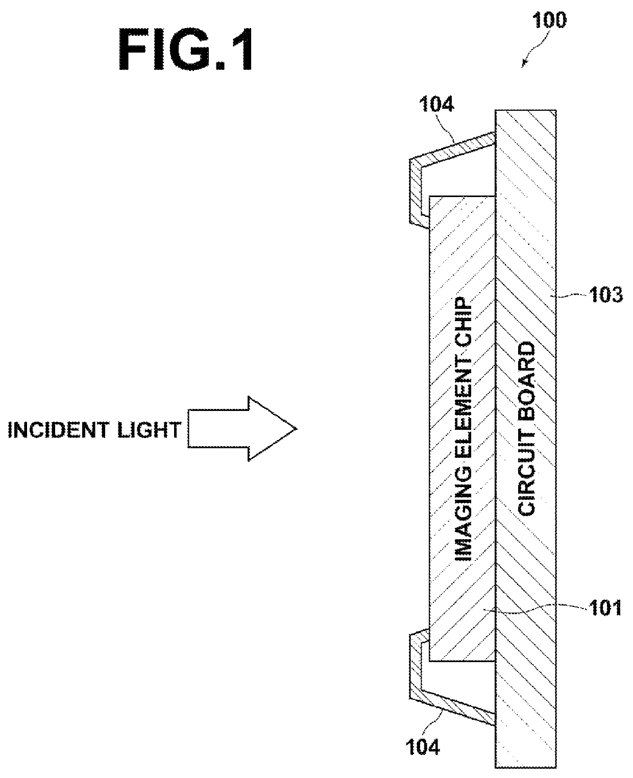
[0068]First, the configuration of a solid-state imaging element 100 will be briefly described. FIG. 1 is a diagram that schematically illustrates the traverse cross section of the solid-state imaging element 100. This solid-state imaging element 100 is equipped with an imaging element chip 101 and a circuit board 103 attached to the back side of the imaging element chip 101.

[0069]An area of the circuit board 103 is larger than that of the imaging element chip 101. The imaging element chip 101 is attached to the center portion of the circuit board 103. Connection pads are formed at a peripheral portion of the imaging element chip 101, i.e., a peripheral portion of an imaging region. Each of the connection pads is bonded to the circuit board 103 by a wire 104.

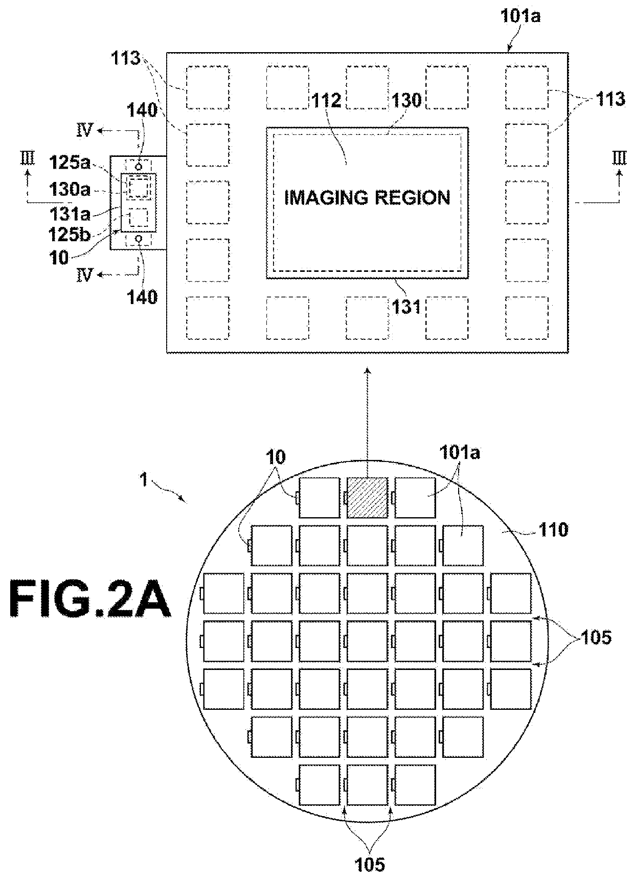
[0070]The imaging element chip 101 is an individual piece formed from a wafer for forming an imaging ...


PUM


Abstract

A wafer for forming an imaging element has a test pattern and a plurality of imaging element units. The wafer has an imaging region which includes a great number of photoelectric conversion pixels, an imaging element units and a test pattern. The test pattern includes a testing organic photoelectric conversion film and a testing counter electrode having the same configuration and formed at the same time as the organic photoelectric conversion film and a counter electrode, respectively of the photoelectric conversion pixels. A first testing terminal is electrically connected to the undersurface side of the testing organic photoelectric conversion film, and a second testing terminal is electrically connected to the testing counter electrode. A protective film is formed over the entire semiconductor wafer so as to cover the imaging region and the test pattern, and is then partially removed so that a part of each testing terminal is exposed.

Description

CROSS-REFERENCE TO RELATED APPLICATIONS[0001]This application is a Continuation of PCT International Application No. PCT / JP2013 / 002010 filed on Mar. 25, 2013, which claims priority under 35 U.S.C. §119(a) to Japanese Patent Application No. 2012-078609 filed on Mar. 30, 2012. The above application(s) is hereby expressly incorporated by reference, in its entirety, into the present application.BACKGROUND OF THE INVENTION[0002]1. Technical Field[0003]The present invention relates to a wafer for forming an imaging element which is generated in the manufacturing process of a solid-state imaging element, a method for manufacturing the solid imaging element, and an imaging element chip.[0004]2. Background Art[0005]In recent years, a solid-state imaging elements, such as an organic CMOS sensor and the like, which includes an organic photoelectric conversion layer at a light receiving portion and the upper portion of which is covered by a protective film, has been proposed as a new solid-stat...

Claims


Application Information

Patent Timeline
Patent Type & Authority Patents(United States)
IPC IPC(8): G01R31/26H01L27/30H01L27/146H01L51/00G01R31/28H01L51/44
CPCH01L27/14603H01L27/307H01L51/0031G01R31/2831G01R31/2884H01L51/441H01L51/448Y02E10/549Y02P70/50H10K39/32H10K71/70H10K30/81H10K30/88H01L27/14H01L27/146H01L27/14636H01L27/148
Inventor ICHIKI, TAKAHIKO
Owner FUJIFILM CORP
Why Eureka
Try Eureka