
Electronic component

a technology of electronic components and components, applied in the direction of electrical apparatus casings/cabinets/drawers, coupling device connections, semiconductor/solid-state device details, etc., can solve the problems of mobile terminal breakdown and cracking in the circuit board, and achieve the effect of reducing the stress produced near the four corners of the circuit board, preventing cracking, and reducing the density of the mounting electrodes on the other principal surface of the circuit board

Active Publication Date: 2016-05-17
MURATA MFG CO LTD
View PDF14 Cites 0 Cited by
  • Summary
  • Abstract
  • Description
  • Claims
  • Application Information

AI Technical Summary

Benefits of technology

[0008]Accordingly, preferred embodiments of the present invention provide a technique capable of effectively preventing a fracture, a chip, and a crack from being caused in a circuit board.
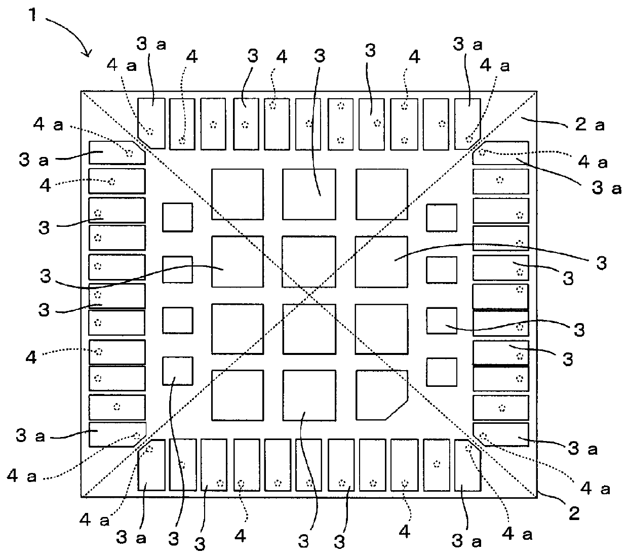
[0010]Preferably, the mounting electrodes near the corners are each shaped like a rectangle whose corner closest to the corresponding diagonal line is cut off. According to this structure, stress produced near the four corners of the circuit board is more effectively reduced, and a fracture, a chip, and a crack can be effectively prevented from being caused in the circuit board. Moreover, the density of the mounting electrodes on the other principal surface of the circuit board can be increased.
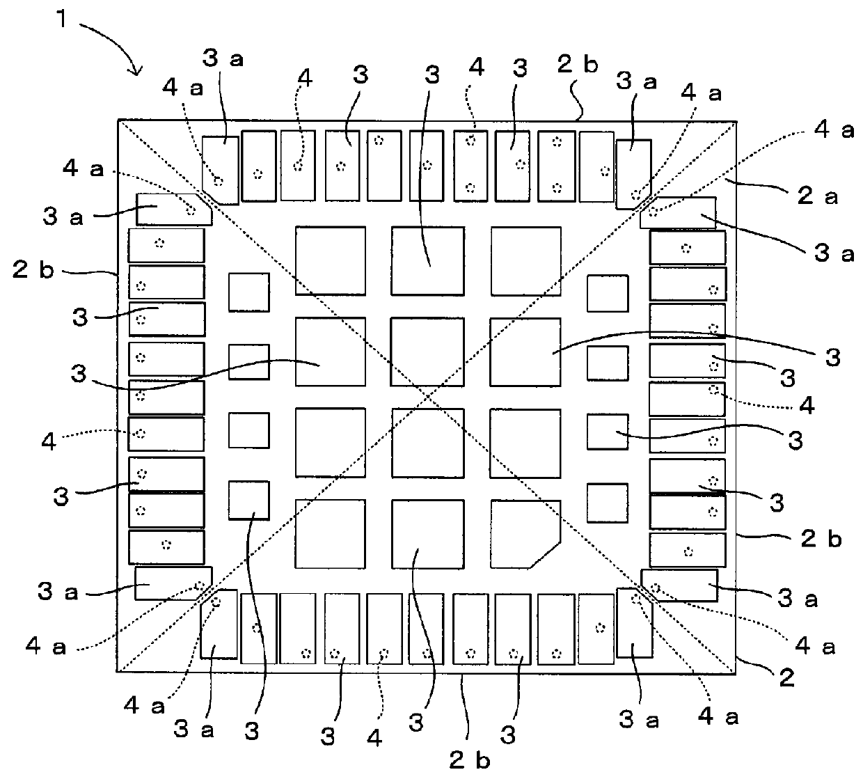
[0011]Preferably, the mounting electrodes near the corners are provided at positions farther from an outer edge of the other principal surface than the other mounting electrodes arranged along the outer edge. According to this structure, the distances between the mounting electrodes near the corners and vertexes of the circuit board are increased, and the stress produced near the corners of the circuit board are further reduced. This can more effectively prevent a fracture, a chip, and a crack from being caused in the circuit board.
[0012]Preferably, the electronic component further includes a plurality of through holes for interlayer connection provided in the circuit board, and the through holes connected to the mounting electrodes near the corners, of the through holes, are provided at positions farthest from the corners of the circuit board. According to this structure, the stress produced between the vertexes of the circuit board and the through holes provided near the corners of the circuit board is effectively reduced, and a fracture, a chip, and a crack can be effectively prevented from being caused in the circuit board.
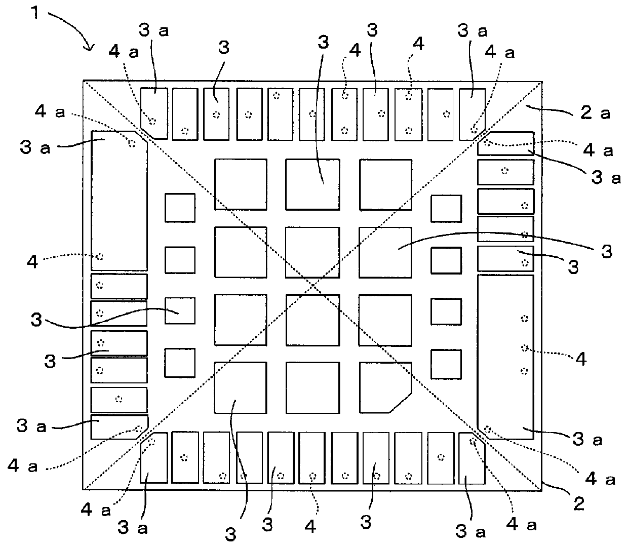
[0013]The mounting electrode near at least one of the corners of the circuit board is preferably longer than the other mounting electrodes in a direction of one side adjacent to the mounting electrode near the at least one of the corners. According to this structure, the contact area between a motherboard and the circuit board is increased, and this can increase the mounting strength.
[0014]According to various preferred embodiments of the present invention, the mounting electrodes near the four corners of the circuit board, of the mounting electrodes provided on the other principal surface of the circuit board included in the electronic component, are provided at the positions shifted from the diagonal lines of the other principal surface. As a result, the stress produced near the four corners of the circuit board is reduced, and this can effectively prevent a fracture, a chip, and a crack from being caused in the circuit board.

Problems solved by technology

This may cause a fracture, a chip, and a crack in the circuit board.
In this case, transmission lines, such as via holes of the circuit board or a wiring pattern provided in the circuit board, may be broken, and this may result in a breakdown of the mobile terminal.

Method used


Image

  • Electronic component
  • Electronic component
  • Electronic component

Examples


first preferred embodiment

[0024]An electronic component according to a first preferred embodiment of the present invention will be described with reference to FIG. 1. FIG. 1 is a bottom view of the electronic component according to the first preferred embodiment of the present invention.

[0025]An electronic component 1 illustrated in FIG. 1 includes a circuit board 2 that preferably is a multilayered ceramic board, in which components, for example, a semiconductor element such as an amplifier, a diode, and a switch including a transistor or an FET, a resistor element, a capacitor element, and an inductor element, are mounted on at least a front surface (one principal surface), and land-shaped surface mounting electrodes 3 and 3a are mounted on a back surface 2a (the other principal surface). The electronic component 1 preferably is a module such as a Bluetooth (registered trademark) module, a wireless LAN module, or an antenna switch module for a cellular phone, for example. The unillustrated front surface of...

second preferred embodiment

[0037]An electronic component according to a second preferred embodiment of the present invention will be described with reference to FIG. 2. FIG. 2 is a bottom view of the electronic component according to the second preferred embodiment of the present invention.

[0038]This preferred embodiment is different from the above-described first preferred embodiment in that, as illustrated in FIG. 2, mounting electrodes 3a near the corners are provided at positions farther from an outer edge 2b of a back surface 2a of a circuit board 2 than other mounting electrodes 3 arranged along the outer edge 2b, that is, at positions closer to the center of the back surface 2a. Since other structures are similar to those adopted in the above-described first preferred embodiment, they are denoted by the same reference numerals, and descriptions thereof are skipped.

[0039]According to this preferred embodiment, since the mounting electrodes 3a near the corners of the circuit board 2 are provided at the p...

third preferred embodiment

[0040]An electronic component according to a third preferred embodiment of the present invention will be described with reference to FIG. 3. FIG. 3 is a bottom view of the electronic component according to the third preferred embodiment of the present invention.

[0041]This preferred embodiment is different from the above-described first preferred embodiment in that, as illustrated in FIG. 3, a mounting electrode 3a near at least one corner is longer than other mounting electrodes 3 in a direction of one side of the circuit board 2 adjacent to the mounting electrode 3a near the corner. Since other structures are similar to those adopted in the above-described first preferred embodiment, they are denoted by the same reference numerals, and descriptions thereof are skipped.

[0042]According to this preferred embodiment, the mounting electrode 3a near at least one corner is longer than the other mounting electrodes 3 in the direction of one side of the circuit board 2 adjacent to the mount...


PUM


Abstract

Based on a result of repeated analysis of stress caused by application of an external impact in a circuit board, which is rectangular or substantially rectangular in plan view and includes mounting electrodes, included in an electronic component, the mounting electrodes near four corners of the circuit board, of the mounting electrodes provided on a back surface of the circuit board included in the electronic component, are provided at positions shifted from diagonal lines of the back surface. Hence, the stress produced near the four corners of the circuit board is reduced, and this can effectively prevent a fracture, a chip, and a crack from being caused in the circuit board.

Description

BACKGROUND OF THE INVENTION[0001]1. Field of the Invention[0002]The present invention relates to an electronic component including a circuit board which is rectangular or substantially rectangular in plan view and in which a component is mounted on at least one principal surface and a plurality of land-shaped mounting electrodes are provided on the other principal surface.[0003]2. Description of the Related Art[0004]In recent years, there has been a demand to further reduce the size of mobile terminals. Also, there has been a demand to further reduce the size and height of electronic components (electronic radio-frequency modules) mounted on motherboards in the mobile terminals, for example, a Bluetooth (registered trademark) module, a wireless LAN module such as a Wi-Fi module, and an antenna switch module for a cellular phone. Such an electronic component includes a circuit board in which components, for example, a semiconductor element such as a transistor, an FET, a diode and an...

Claims


Application Information

Patent Timeline
Patent Type & Authority Patents(United States)
IPC IPC(8): H05K1/11H01L23/498H01R13/56H05K3/34
CPCH01R13/56H01L23/49838H05K1/112H01L2924/0002H05K3/3436H01L2924/00
Inventor AOYAMA, YOSHIHIROSHIMAKAWA, JUNYA
Owner MURATA MFG CO LTD
Learn More