Wafer-level die to package and die to die interconnects suspended over integrated heat sinks

a technology of heat sink and package die, which is applied in the direction of solid-state devices, basic electric elements, electric apparatus construction details, etc., can solve the problem of difficulty in pairing modern ics with pins

Active Publication Date: 2016-07-05
HRL LAB
View PDF42 Cites 36 Cited by
  • Summary
  • Abstract
  • Description
  • Claims
  • Application Information

AI Technical Summary

Benefits of technology

[0007]In one aspect the present invention provides an interconnect for electrically coupling pads formed on adjacent chips or on packaging material adjacent said chips, with an electrically conductive heat sink disposed between said pads, the interconnect comprising:

Problems solved by technology

Wire bonds, while seemingly small, with the continued tend for smaller and smaller device geometries, the wire bonds now are so large compared with the device geometries of modern integrated c

Method used


Image

  • Wafer-level die to package and die to die interconnects suspended over integrated heat sinks
  • Wafer-level die to package and die to die interconnects suspended over integrated heat sinks
  • Wafer-level die to package and die to die interconnects suspended over integrated heat sinks

Examples


Embodiment Construction

[0015]This technology of U.S. Pat. No. 8,617,927 teaches how microelectronic integrated circuits (ICs—also referred to as “chips” and “dice” herein) may be embedded in thermal heat sinks or heat spreaders at the wafer level. This patent application teaches an improved technique for interconnecting at the wafer level either multiple chips and / or for connecting one or more chips to pins associated with wafer packaging material which preferably supports or houses one or more such chips and one or more heat sinks (which also called heat spreaders herein).

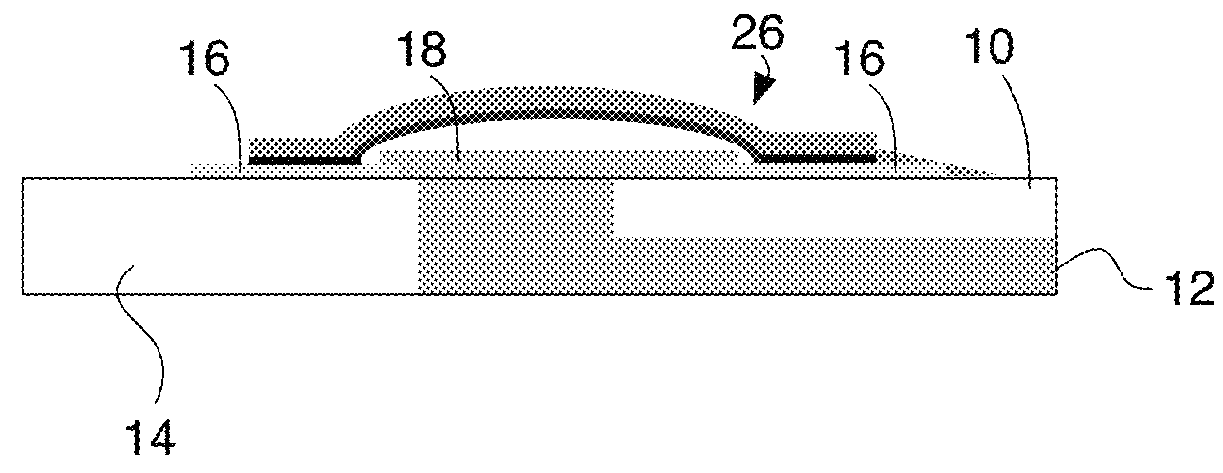
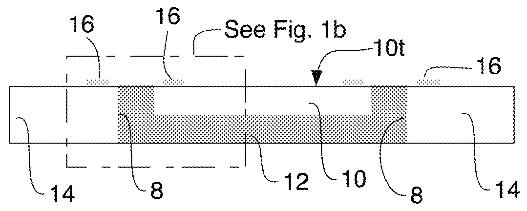
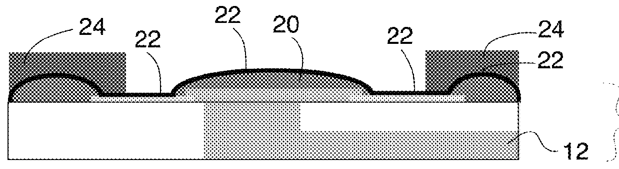
[0016]FIG. 1a shows an active integrated circuit die or chip 10 embedded in a heat sink or heat spreader 12 which in turn is embedded in wafer packaging material 14. FIG. 1b depicts in greater detail the portion of FIG. 1a within the broken line (and shows, as is discussed below, an initial step utilized in forming a suspended interconnect). FIG. 1c-1f depict additional stages in the fabrication of a suspended die-to-package interconnec...


PUM


Abstract

An interconnect for electrically coupling pads formed on adjacent chips or on packaging material adjacent the chips, with an electrically conductive heat sink being disposed between the pads, the interconnect comprising a metallic membrane layer disposed between two adjacent pads and disposed or bridging over the electrically conductive heat sink so as to avoid making electrical contact with the electrically conductive heat sink. An electroplated metallic layer is disposed on the metallic membrane layer. Fabrication of interconnect permits multiple interconnects to be formed in parallel using fabrication techniques compatible with wafer level fabrication of the interconnects. The interconnects preferably follow a smooth curve to electrically connect adjacent pads and following that smooth curve they bridge over the intervening electrically conductive heat sink material in a predictable fashion.

Description

STATEMENT REGARDING FEDERALLY SPONSORED RESEARCH OR DEVELOPMENT[0001]This invention was made under US Government contact number FA8650-11-C-7181 and therefore the US Government may have certain rights to this invention.CROSS REFERENCE TO RELATED APPLICATIONS[0002]This application is related to U.S. Pat. No. 8,617,927 which is hereby incorporated herein by reference.TECHNICAL FIELD[0003]A technology to connect an active circuit die or chip embedded in a thermal heat spreader to other dice or chips or circuit connectors adjacent or near the thermal heat spreader and integrated into a substrate at the wafer level.BACKGROUND[0004]U.S. Pat. No. 8,617,927 teaches a method of mounting electronic dice or chips into an electroformed heat spreader. Of course, the dice or chips either need to be interconnected with each other or connected to pins or connectors associated with the packaging material used to support or house the dies or chips and their heat sinks (also called heat spreaders here...

Claims


Application Information

Patent Timeline
IPC IPC(8): H01L21/00H01L23/532H05K7/20H01L21/768H01L23/36H01L23/528H01L23/10
CPCH01L23/528H01L23/36H01L21/76873H01L23/53247H01L21/76829H01L21/76816H01L21/76877H05K7/20154H01L21/568H01L24/16H01L24/19H01L24/20H01L24/24H01L24/82H01L24/96H01L25/105H01L2224/04105H01L2224/12105H01L2224/16227H01L2224/24137H01L2225/1035H01L2225/1058H01L2225/1094H01L2924/10253H01L2924/10271H01L2924/1033H01L2924/10335H01L2924/14H01L2924/15153H01L2924/15311H01L23/147H01L23/367H01L23/49822H01L23/5389H01L21/0273H01L21/2885H01L21/6835H01L23/3675H01L23/3736H01L24/17H01L24/64H01L24/70H01L24/89H01L25/16H01L25/18H01L25/50H01L2224/13023H01L2224/13109H01L2224/13111H01L2224/13113H01L2224/13116H01L2224/13139H01L2224/13144H01L2224/13147H01L2224/13155H01L2224/13157H01L2924/01022H01L2924/01079H01L2924/014H01L2924/05042H01L2924/05432H01L2924/06H01L2924/13064H01L2924/13091
Inventor HERRAULT, FLORIAN G.YAJIMA, MELANIE S.MARGOMENOS, ALEXANDROSMICOVIC, MIROSLAV
Owner HRL LAB
Why Eureka
Try Eureka