Semiconductor processing reactor and components thereof

a technology of semiconductors and reactors, applied in the direction of chemical vapor deposition coatings, transportation and packaging, coatings, etc., can solve the problem of non-uniform deposition on the substra

Active Publication Date: 2016-07-19
ASM IP HLDG BV
View PDF1180 Cites 364 Cited by
  • Summary
  • Abstract
  • Description
  • Claims
  • Application Information

AI Technical Summary

Benefits of technology

[0012]Advantages of the present invention will become more apparent to those skilled in the art from the following description of the embodiments of the invention which have been shown and described by way of illustration. As will be realized, the invention is capable of other and different embodiments, and its details are capable of modification in various respects. Accordingly, the drawing(s) and description are to be regarded as illustrative in nature and not as restrictive.

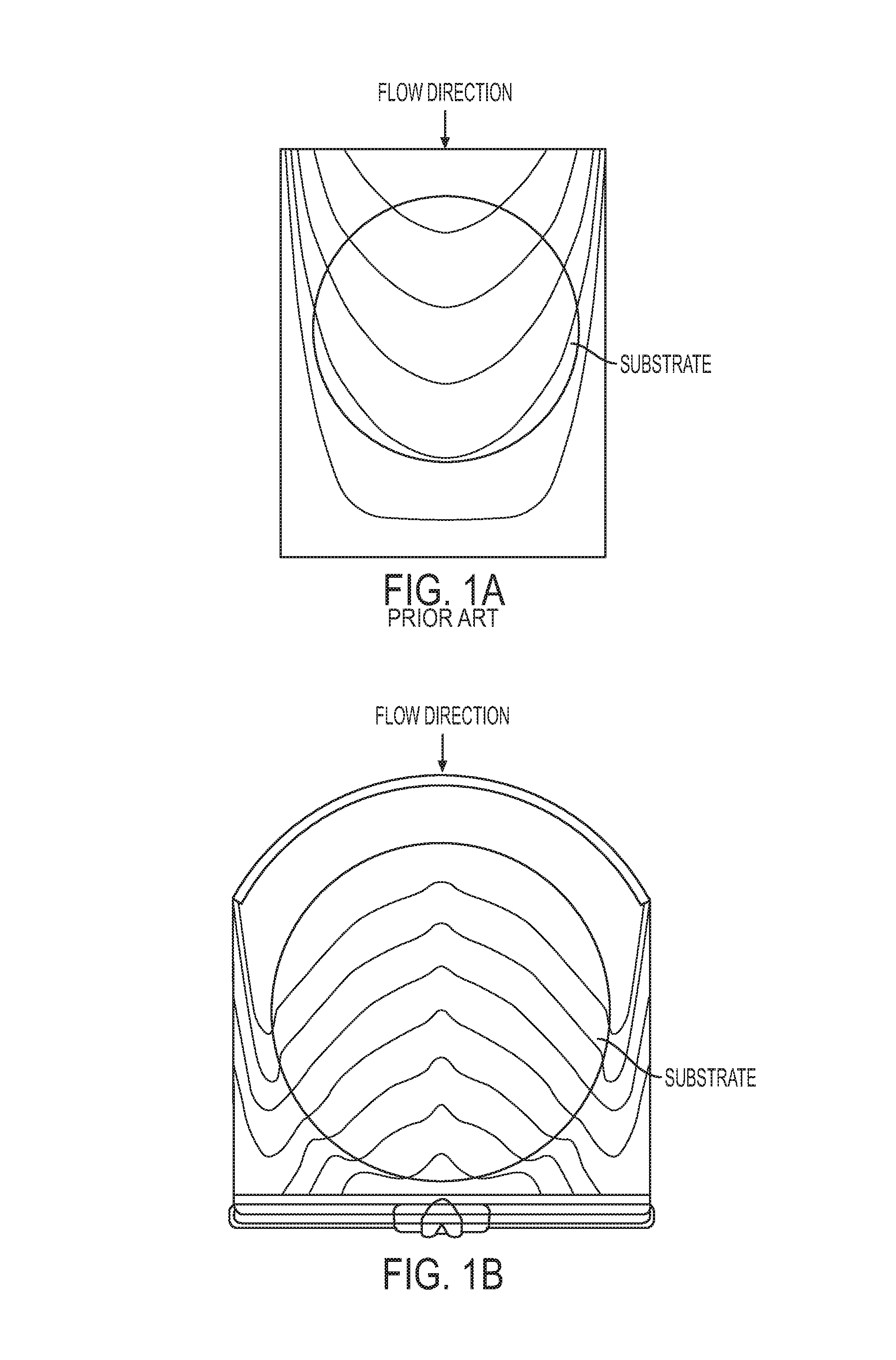
Problems solved by technology

The decrease in precursor concentration within the process gases flowing over the substrate from the leading to the trailing edge of the substrate—and a similar decrease in concentration from the longitudinal centerline relative to the side edges of the reaction chamber—results in non-uniform deposition on the substrate.

Method used


Image

  • Semiconductor processing reactor and components thereof
  • Semiconductor processing reactor and components thereof
  • Semiconductor processing reactor and components thereof

Examples


Embodiment Construction

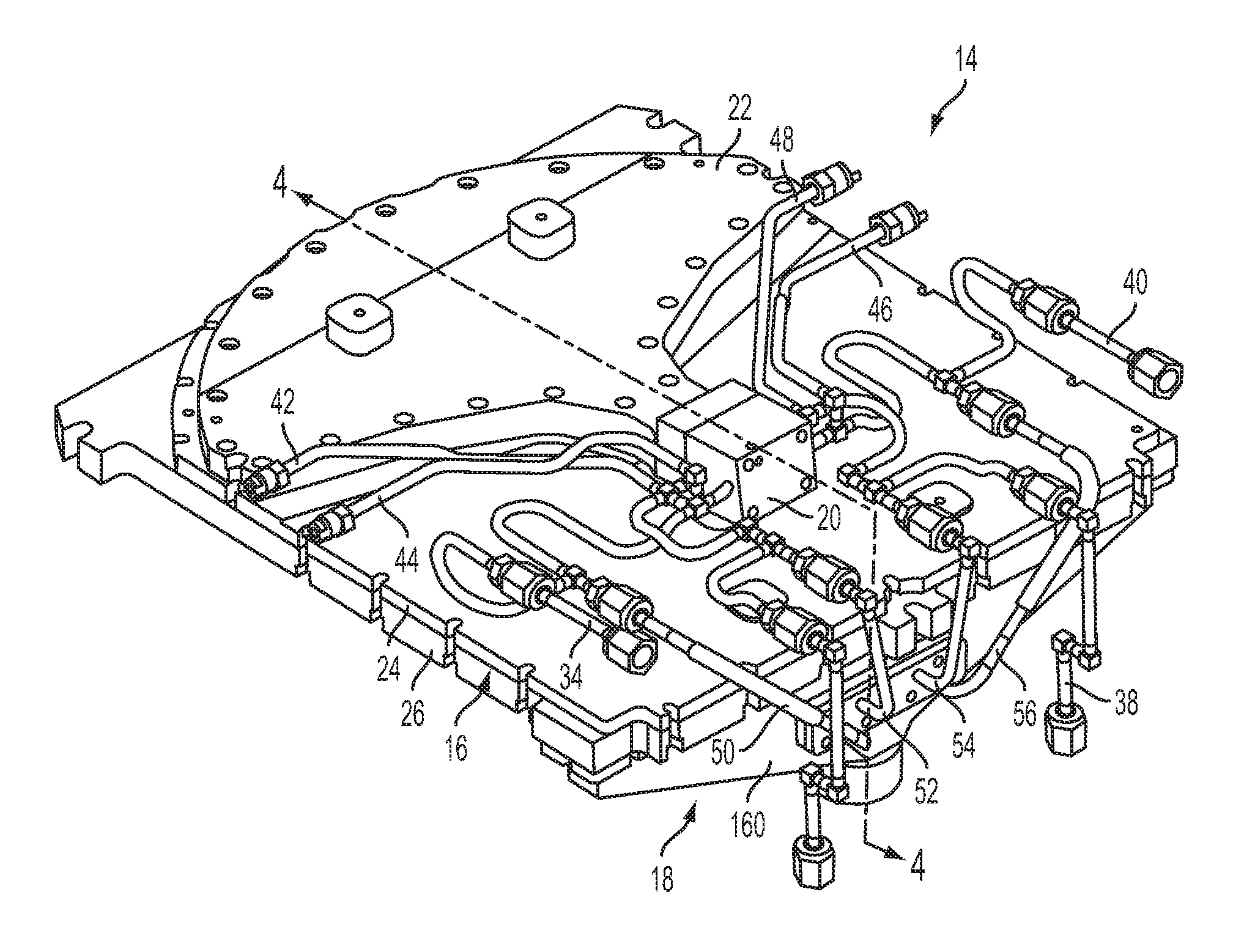
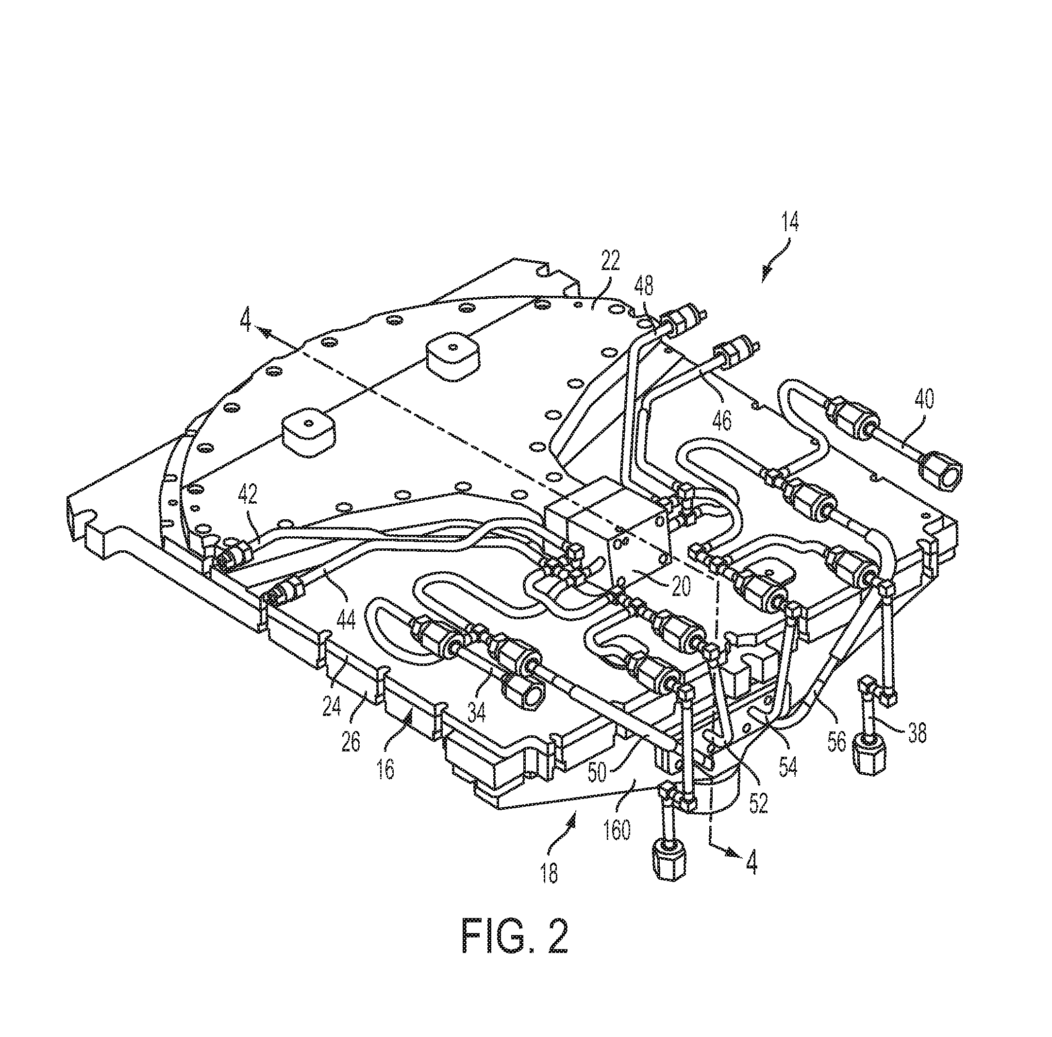
[0034]Referring to FIGS. 2-4, an exemplary embodiment of a reactor 10 for use in a semiconductor processing tool is shown. The reactor 10 includes a housing 12, a gas delivery system 14, a reaction chamber 16, and an exhaust assembly 18. The housing 12 forms a chamber in which a semiconductor substrate can be processed. The reactor 10 is configured to receive a semiconductor substrate that is inserted into the reaction chamber 16. Once in the reaction chamber 16, any number of different processes and chemical reactions can be performed on the substrate including an etching process, a film deposition process, a baking process, or any other process known to one of ordinary skill in the art. After the substrate is processed within the reaction chamber 16, the substrate is removed, and another substrate can then be inserted into the reaction chamber 16 to be processed. In an embodiment, the housing 12 provides a reduced pressure chamber in which the processing components reside. In anot...


PUM

PropertyMeasurementUnit
distanceaaaaaaaaaa
distanceaaaaaaaaaa
distanceaaaaaaaaaa

Abstract

A reactor having a housing that encloses a gas delivery system operatively connected to a reaction chamber and an exhaust assembly. The gas delivery system includes a plurality of gas lines for providing at least one process gas to the reaction chamber. The gas delivery system further includes a mixer for receiving the at least one process gas. The mixer is operatively connected to a diffuser that is configured to diffuse process gases. The diffuser is attached directly to an upper surface of the reaction chamber, thereby forming a diffuser volume therebetween. The diffuser includes at least one distribution surface that is configured to provide a flow restriction to the process gases as they pass through the diffuser volume before being introduced into the reaction chamber.

Description

CROSS-REFERENCE TO RELATED APPLICATIONS[0001]The present application claims priority under 35 U.S.C. 119(e) to U.S. Provisional Patent Application No. 61 / 167,093, filed Apr. 6, 2009.FIELD OF THE INVENTION[0002]The present application relates generally to semiconductor processing equipment and specifically to an apparatus and system for delivering process gases to a substrate reaction chamber.BACKGROUND OF THE INVENTION[0003]Atomic layer deposition (“ALD”) is a well known process in the semiconductor industry for forming thin films of materials on substrates such as silicon wafers. ALD is a type of vapor deposition wherein a film is built up through deposition of multiple ultra-thin layers with the thickness of the film being determined by the number of layers deposited. In an ALD process, gaseous molecules of one or more compounds (precursors) of the material to be deposited are supplied to the substrate or wafer to form a thin film of that material on the substrate. In one pulse, a...

Claims


Application Information

Patent Timeline
Patent Type & Authority Patents(United States)
IPC IPC(8): C23C16/455
CPCC23C16/45544C23C16/45502C23C16/45504C23C16/45525C23C16/45561C23C16/45591Y10T137/85938H01L21/0228H01L21/02296H01L21/205
Inventor SHERO, ERICVERGHESE, MOHITH E.WHITE, CARL L.TERHORST, HERBERTMAURICE, DAN
Owner ASM IP HLDG BV
Why Eureka
Try Eureka