
Integrated ingot for TSV substrates and method for making the same

a technology of integrated ingots and substrates, applied in semiconductor devices, thin material processing, semiconductor/solid-state device details, etc., to achieve the effect of small via diameter, fine via pitch and efficient production

Active Publication Date: 2016-07-19
IC CHIP COOLING TECH LLC
View PDF3 Cites 4 Cited by
  • Summary
  • Abstract
  • Description
  • Claims
  • Application Information

AI Technical Summary

Benefits of technology

The present invention allows for efficient production of TSV substrates in a batch way and allows for precise placement of other additive elements such as capacitors, resistors, and inductors. The invention also allows for very small via diameter and very fine via pitch using very thin metal wires. The key invention concepts involve using a precise patterned array of metal wires and integrating other additive elements into the patterned array, which results in an integrated ingot. These features provide improved efficiency and precision in the production of TSV substrates.

Problems solved by technology

Because a great amount of metal wires and a great amount of discrete additive elements may be involved in the production of an integrated ingot, it is a challenge to precisely arrange and fix these great amount of metal wires and additive elements to form a patterned array of metal wires and additive elements at desired location.

Method used


Image

  • Integrated ingot for TSV substrates and method for making the same
  • Integrated ingot for TSV substrates and method for making the same
  • Integrated ingot for TSV substrates and method for making the same

Examples


Embodiment Construction

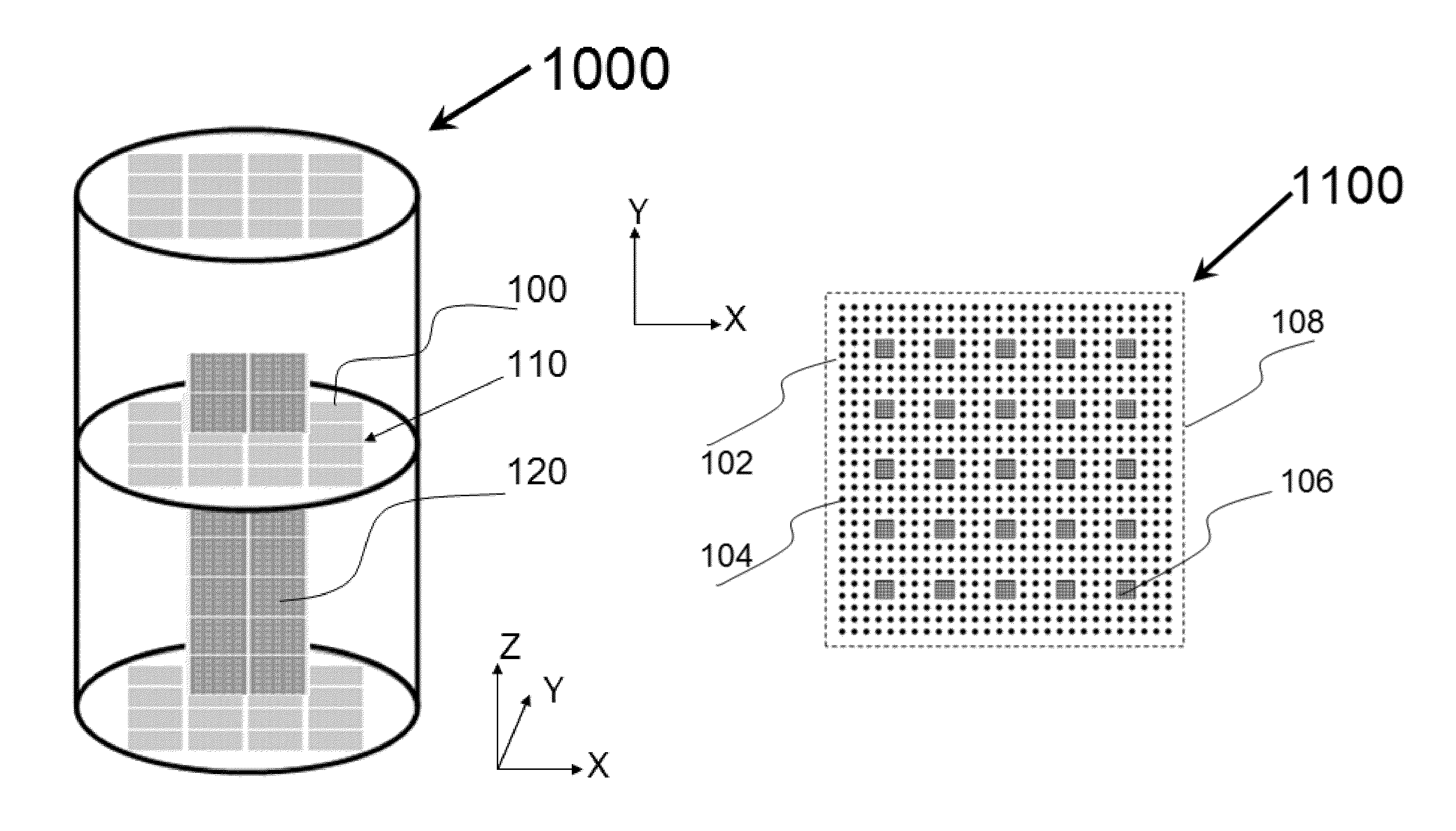
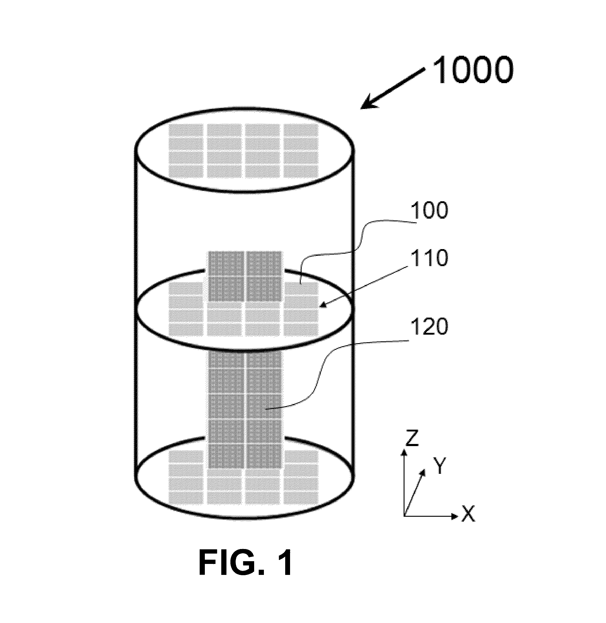
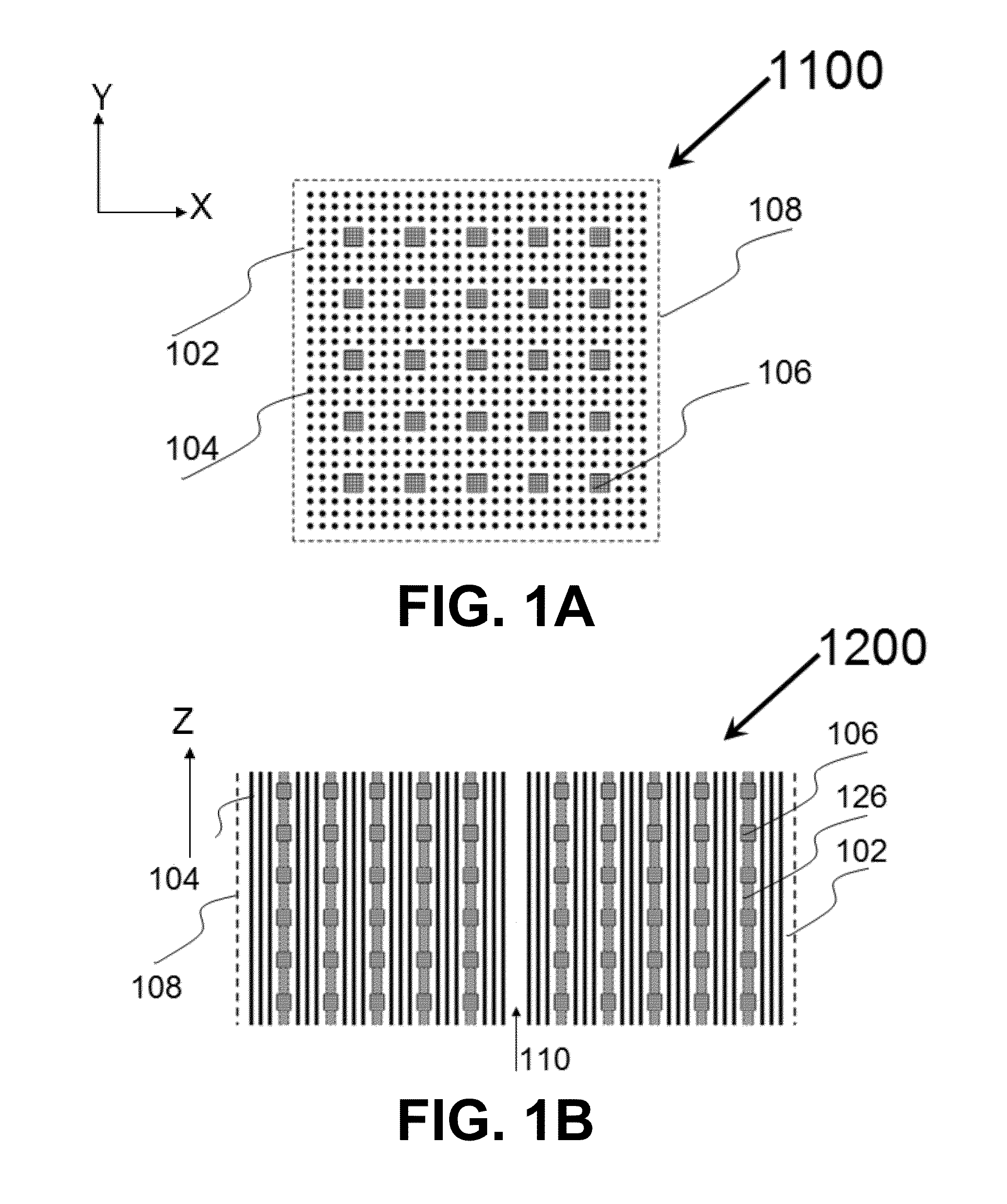
[0029]Some terminologies used in the detailed descriptions are first explained herein for illustrative clarity. 1): A patterned array of metal wires means that the cross-sections of these metal wires form a patterned array. The difference between a patterned array of metal wires and an array of metal wires is that a patterned array may have more features in addition to an array which only include a regular arrangement in X and Y direction. An example of a patterned array of metal wires is an array of metal wires with the feature of sawing streets as showed in FIG. 1. The sawing streets separate an array of metal wires into a plurality of units in X and Y directions, and each unit contains an array of metal wires. Another example of a patterned array of metal wires is a depopulated array of metal wires wherein some metal wires are removed from the array of metal wires as showed in FIG. 1C. 2): An additive element means something else in contrast to metal wires, particularly means a p...


PUM

PropertyMeasurementUnit
sizeaaaaaaaaaa
diameteraaaaaaaaaa
diameteraaaaaaaaaa

Abstract

The disclosure describes a metal-wire-based method for making an integrated ingot, which basically comprises a dielectric matrix and a patterned array of metal wires, and may further comprise other additive elements at desired locations. After sawing the integrated ingot into slices, a plurality of substrates containing through substrate metal pillars and other additive elements at desired locations are produced in a batch way. The metal-wire-based method comprises the key steps: forming a patterned array of metal wires, precisely integrating other additive elements at desired locations when needed, forming a solid dielectric material in the empty space among and around metal wires and other additive elements. Furthermore, a guidance metal wire method is described for precisely integrating other additive elements at desired locations in a patterned array of metal wires.

Description

TECHNICAL FIELD OF THE INVENTION[0001]The disclosure relates generally to 3-dimensional (3D) integrated circuit semiconductor packaging technology, and particularly to technologies for producing through silicon via (TSV), through substrate via (TSV) and through glass via (TSV) interposers, which are used in packaging semiconductor chips or electric devices.BACKGROUND OF THE INVENTION[0002]An interposer is a bridge connecting two or more electric devices with a fine pitch of electric contact pads to a substrate or board with a coarse pitch of electric contact pads. Through silicon via (TSV) is a vertical electrical connection completely through a silicon wafer or die. A silicon TSV interposer may connect multiple chips with fine pitch mounted on its top side to a substrate with a coarse pitch. A silicon TSV interposer may also connect chips mounted on its both sides. A silicon TSV interposer basically comprises a silicon substrate with TSVs and redistribution layers (RDL) and electri...

Claims


Application Information

Patent Timeline
Patent Type & Authority Patents(United States)
IPC IPC(8): H01L29/40H01L21/44H01L23/52H01L23/498H01L21/48
CPCH01L23/49827H01L21/486H01L21/4842H01L23/49838H01L23/49866H01L23/49894H01L2924/0002Y10T428/24802Y10T29/49162H01L2924/00
Inventor SHEN, YUCI
Owner IC CHIP COOLING TECH LLC
Learn More