Crossed-dipole antenna array structure

a technology of antenna array and dipole antenna, which is applied in the direction of antennas, antenna feed intermediates, antenna details, etc., can solve the problems of increasing the problem of diagonally between the two cards, establishing a crossing dipole substantially perpendicular to the dipole card using a conventional “cross brace” with attached ends, and promoting perpendicularity, so as to reduce the spacing between the crossed dipoles and related structures , the effect of promoting perpendicular

Active Publication Date: 2016-07-19
FIRST RF CORP
View PDF18 Cites 16 Cited by
  • Summary
  • Abstract
  • Description
  • Claims
  • Application Information

AI Technical Summary

Benefits of technology

[0008]Another embodiment of the structure particularly addresses a problem that becomes more prevalent as the operating frequency at which the crossed-dipoles operate increases. To elaborate, as the operating frequency increases, the size of the crossed-dipoles and related structures decreases. Moreover, in an array of crossed-dipoles, the spacing between the crossed-dipoles decreases as the operating frequency range increases. For example, in a crossed-dipole antenna designed to operate in the Ku band (14-16 GHz for data links), the distances between the ends of the radiating elements of one dipole of a crossed-dipole and between immediately adjacent crossed-dipoles are typically on the order of 9-10 mm. With such small structures and distances between adjacent crossed-dipole antennas, establishing a crossing dipole card substantially perpendicular to a dipole card using a conventional “cross brace” with ends that are attached to the two cards and that extends diagonally between the cards becomes increasing problematic. In this embodiment, the cross-dipole antenna array structure employs a dipole card and crossing dipole cards that supplement notches which allow an “egg crating” engagement between the cards with at least two rails that are disposed parallel to each intersection line defined by the engagement of dipole card and one of the crossing dipole cards. Each of the rails is associated with one of the dipole card and the crossing dipole card, extends away from the surface of the card, and engages a surface associated with the other card in a manner that promotes perpendicularity between the dipole card and the crossing dipole card. In a particular embodiment, four rails are disposed parallel to each intersection line defined by the engagement of the dipole card and one of the crossing dipole cards. Each of the rails is located in a separate corner. By having a rail in each corner, a high degree of perpendicularity can be established between the dipole card and each of the crossing dipole cards. In one embodiment, each of the rails is also electrically conductive and a portion of one of the dipole antenna and crossing dipole antenna that form a crossed-dipole. Consequently, the rails serve both to facilitate perpendicularity between the dipole card and the crossing dipole card and to function as part of a crossed-dipole antenna. In yet a further embodiment, each of the rails is electrically conductive, a portion of one of the dipole antenna and crossing dipole antenna that form a crossed-dipole antenna, and provides a solder surface for establishing one of the multiple solder joints. As such, the rails serve to facilitate perpendicularity between the cards, function as part of a crossed-dipole antenna, provide solder surfaces that, if used, substantially fix the perpendicularity established by the interaction of the rails and the card surfaces, and establish electrical connections between the crossing dipole and the feed circuitry located on the dipole card.
[0009]Yet another embodiment that addresses the problem of establishing substantial perpendicularity between the crossing dipole cards and the dipole card supplements notches which allow an “egg crating” engagement between the cards with a tab-and-hole structure. In a particular embodiment, a plurality of holes are defined by the dipole card with each hole located along one of the intersection lines defined by the engagement of the dipole card and each one of the crossing dipole cards. The crossing dipole card has an edge that defines a tab located to engage one of the holes and, in so doing, establish a substantially perpendicular relationship between the crossing dipole card and the dipole card. The solder joints subsequently established further solidify the perpendicular arrangement. It should be appreciated that a structure in which a crossing dipole card defines a hole that is occupied by a tab defined by the edge of the dipole card is also feasible in many instances. The use of the tab-and-hole structure in combination with the “egg crating” structure to establish perpendicularity between the cards is typically more useful in crossed-dipole arrays that operating at lower frequencies (i.e., below the Ku band) where the dimensions of the crossed-dipoles and the distances between adjacent crossed-dipole are greater. Nonetheless, the tab-and-hole structure can also be used in combination with a rail structure to establish the needed perpendicularity between the cards.
[0010]Another embodiment of the crossed-dipole antenna array structure includes a heat sink for dissipating heat produced by the power amplifier / amplifiers that is / are associated with each crossed-dipole antenna in the array. The feed circuitry for the crossed-dipole antennas is laid out on the dipole card so as to lie to one side of the reflector surface, the dipole antennas being established on the other side of the reflector surface. The power amplifier(s) that are part of the feed circuitry for each of the dipole and crossing dipole antennas is / are established on one side of the dipole card, on the portion of the dipole card that is located to the one side of the reflector surface that is associated with the feed circuitry, and on the portion of the dipole card that is relatively close to the location of the reflector surface. The heat sink includes a pair of planar surfaces that are perpendicular to one another. One of these planar surfaces is connected to the other side of the dipole card (i.e., the side of the dipole card that does not support the power amplifier(s) for a crossed-dipole or multiple crossed-dipoles) and substantially opposite to the locations of the power amplifiers so as to establish a thermal circuit between the power amplifiers and the heat sink. The other planar surface of the heat sink is thermally connected to the reflector to allow heat produced by the power amplifiers to be transmitted by the heat sink to the reflector and then dissipated by the reflector. In a particular embodiment, the reflector is comprised of multiple pieces that are both perpendicular to the dipole card and sandwich the dipole card such that the crossed-dipole antennas are located to one side of the reflector and the feed circuitry (including the power amplifiers) is located to the other side of the reflector. In this embodiment, the other planar surface of the heat sink is thermally connected to one of the two pieces of the reflector. This provides a modular structure comprised of the dipole card with the plurality of crossing dipole cards, a heat sink, and a portion of the reflector that can be readily inserted to and removed from the frame.

Problems solved by technology

With such small structures and distances between adjacent crossed-dipole antennas, establishing a crossing dipole card substantially perpendicular to a dipole card using a conventional “cross brace” with ends that are attached to the two cards and that extends diagonally between the cards becomes increasing problematic.

Method used


Image

  • Crossed-dipole antenna array structure
  • Crossed-dipole antenna array structure
  • Crossed-dipole antenna array structure

Examples


Embodiment Construction

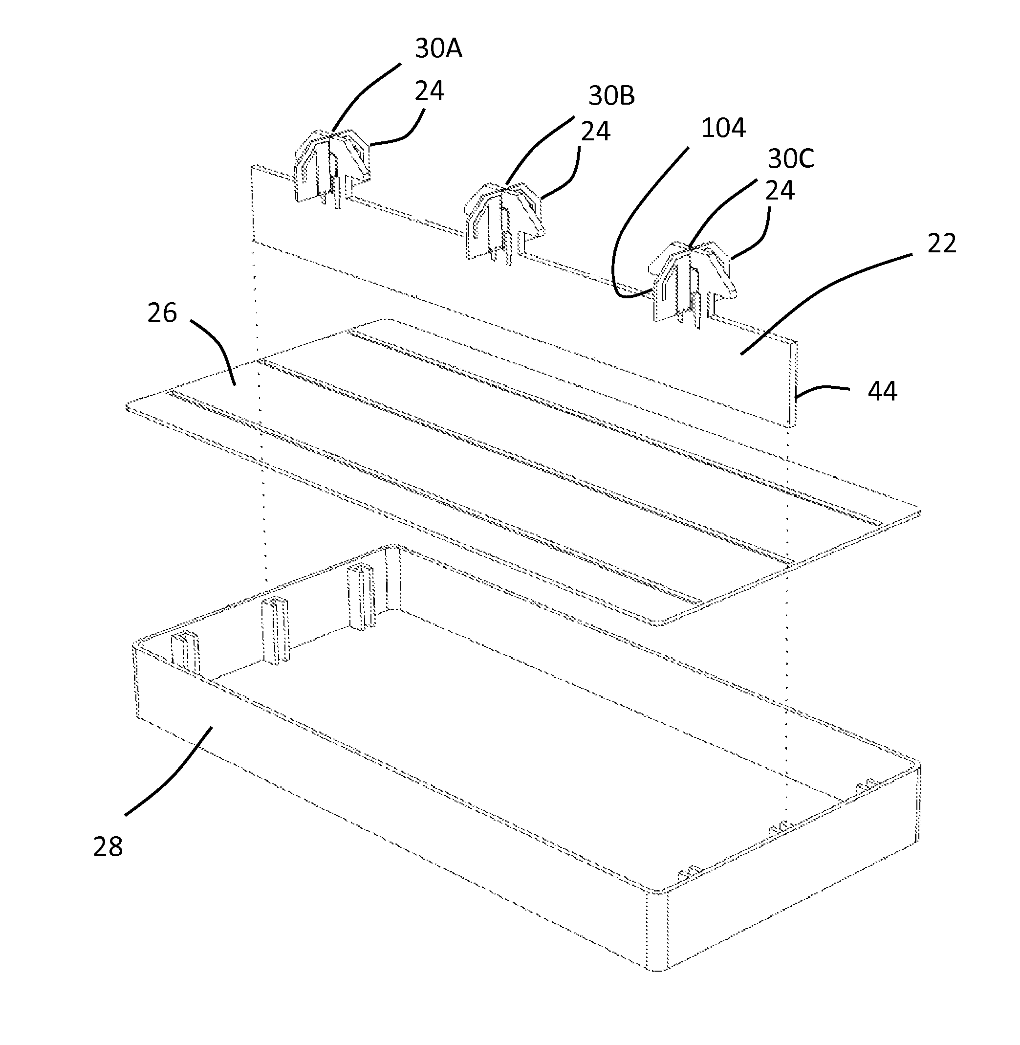
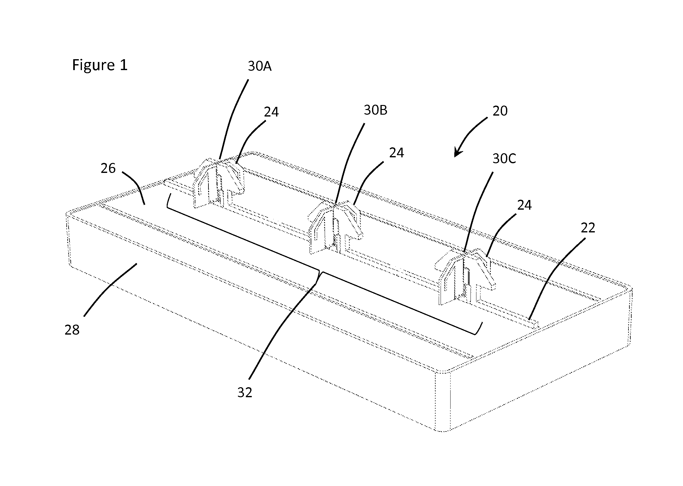
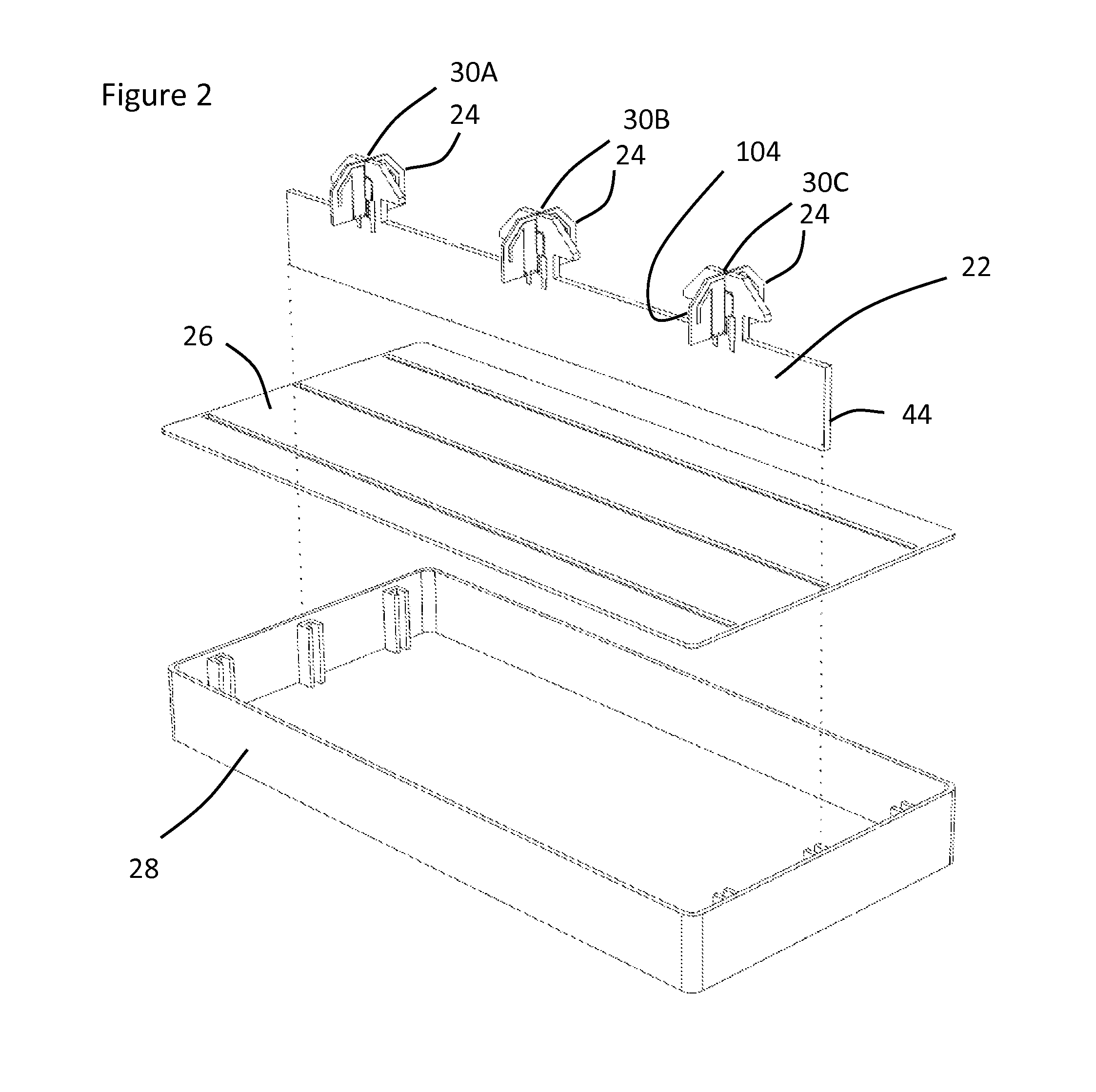
[0031]With reference to FIGS. 1 and 2, an embodiment of a crossed-dipole antenna array structure 20 (hereinafter structure 20) is described. Generally, the structure 20 is comprised of a dipole card 22, a plurality of crossing dipole cards 24, a reflector 26, and a frame 28.

[0032]The dipole card 22 supports a plurality of dipole antennas. Each of the crossing dipole cards 24 supports a substantial portion of a crossing dipole antenna. Additionally, each of the crossing dipole antenna cards 24 is disposed substantially perpendicular to the dipole card 22 and, when operatively associated with the dipole card 22, establishes one of a plurality of crossed-dipole antennas 30A-30C formed from one of the dipole antennas on the dipole card 22 and the substantial portion of the crossing dipole antenna associated with the crossing dipole card 24. The operative association of all of the crossing dipole cards 24 with the dipole card 22 produces an array of crossed-dipole antennas 32. The reflec...


PUM


Abstract

The invention is directed to a crossed-dipole antenna structure that, in one embodiment, is comprised of: (a) a first planar dielectric substrate with a feed portion and an antenna portion that supports a first dipole antenna and (b) a second planar dielectric substrate that supports a second dipole antenna or substantial portion of such an antenna. The first and second planar dielectric substrates are positioned substantially perpendicular to one another and so as to form a crossed-dipole antenna from the first and second dipole antennas. The feed portion of the first planar dielectric substrate is electrically and mechanically connected to the second planar substrate by a plurality of solder joints established in the corners defined by the intersections of the first and second planar dielectric substrates.

Description

FIELD OF THE INVENTION[0001]The invention relates to a crossed dipole antenna array structure in which one planar dielectric substrate supports one dipole of a crossed dipole and a second planar dielectric substrate supports the other dipole of the crossed-dipole and the feed circuitry / electronics for both of the dipoles.BACKGROUND OF THE INVENTION[0002]Generally, a crossed-dipole antenna includes a first dipole with a first pair of radiating elements that are in some fashion oriented in or about a first plane and a second dipole with a second pair of radiating elements that are oriented in or about a second plane that is substantially perpendicular to the first plane. The radiating elements can be any of a number of different types (e.g., wires, triangles, spades etc.). Typically, all of the radiating elements in a crossed-dipole are of the same type.[0003]In one type of crossed-dipole antenna, a first dipole is established on a first planar dielectric substrate and a second dipole...

Claims


Application Information

Patent Timeline
Patent Type & Authority Patents(United States)
IPC IPC(8): H01Q21/26H01Q9/16
CPCH01Q9/16H01Q1/246H01Q21/08H01Q21/26
Inventor MCDEVITT, SEAN P.RUMSEY, IAN S.MRUK, JOSEPHKELLY, P. KEITH
Owner FIRST RF CORP
Why Eureka
Try Eureka