

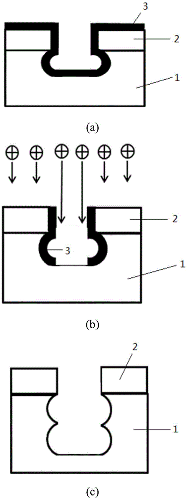
Deep silicon etching method
A technology of deep silicon etching and etching time, applied in coatings, microstructure devices, microstructure technology, etc., can solve the problem that the verticality and roughness of the sidewall are difficult to control, the large etching depth is difficult to achieve, and the etching groove is difficult to achieve. The problem of high verticality of the sidewall can reduce the physical bombardment, reduce the etching depth and increase the etching depth
- Summary
- Abstract
- Description
- Claims
- Application Information
AI Technical Summary
Problems solved by technology
Method used
Image

Examples
Embodiment 1
[0032] The deep silicon etching method comprises the following steps:
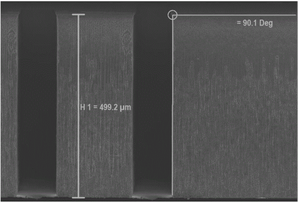
[0033] (1) Prepare an 8 μm thick patterned photoresist mask on the surface of a 500 μm thick silicon wafer.
[0034] (2) Perform deep inductively coupled plasma dry etching on the silicon wafer, including four etching stages.
[0035] (2-1) The first etching stage: three steps of passivation, bombardment and etching are used for 400 times of alternate cycle processing, and the etching depth is 180 μm. The schematic diagram of the process flow of a single cycle is as follows: figure 1 shown.
[0036] Among them, the process parameters of the passivation step are: ion source power 2000W, lower electrode power 0W, cavity air pressure 90mtorr, C 4 f 8 Flow 250sccm, SF 6 The flow rate is 20sccm, and the time is 0.40s.
[0037] The process parameters of the bombardment step are: ion source power 3000W, lower electrode power 75W, cavity air pressure 30mTorr, C 4 f 8 Flow 20sccm, SF 6 The flow rate is 250...
Embodiment 2
[0053] The deep silicon etching method comprises the following steps:
[0054] (1) Prepare a 5 μm thick patterned photoresist mask on the surface of a 350 μm thick silicon wafer.
[0055] (2) Perform deep inductively coupled plasma dry etching on the silicon wafer, including four etching stages.
[0056] (2-1) The first etching stage: three steps of passivation, bombardment and etching are used for 400 times of alternating cycle processing, and the etching depth is 120 μm.
[0057] Among them, the process parameters of the passivation step are: ion source power 1500W, lower electrode power 0W, cavity air pressure 50mTorr, C 4 f 8 Flow 150sccm, SF 6 The flow rate is 0sccm, and the etching time is 0.375s.
[0058] The process parameters of the bombardment step are: ion source power 2000W, lower electrode power 50W, cavity air pressure 15mTorr, C 4 f 8 Flow 0sccm, SF 6 The flow rate is 100sccm, and the etching time is 0.6s.
[0059] The process parameters of the etching s...
PUM
| Property | Measurement | Unit |
|---|---|---|
| depth | aaaaa | aaaaa |
| depth | aaaaa | aaaaa |
| depth | aaaaa | aaaaa |
Abstract
Description
Claims
Application Information