Bulk silicon machining process based on silicon chip etching and puncturing
What is AI technical title?
AI technical title is built by Patsnap AI team. It summarizes the technical point description of the patent document.
A processing technology, silicon wafer technology, applied in the process of producing decorative surface effects, metal material coating process, decorative arts, etc. To eliminate the load effect, increase the sensitive mass, and improve the selection ratio
Active Publication Date: 2014-07-02
HUAZHONG UNIV OF SCI & TECH
View PDF7 Cites 10 Cited by
Summary
Abstract
Description
Claims
Application Information
AI Technical Summary
This helps you quickly interpret patents by identifying the three key elements:
Problems solved by technology
Method used
Benefits of technology
Problems solved by technology
However, limited by the process conditions at this stage, the etch depth of bulk processing generally stays at a shallow stage relative to the thickness of the silicon wafer. When the depth is large, it is difficult to process, and it is difficult to obtain good sidewall roughness and vertical thickness. Spend
Method used
Image
Click on the blue label to locate the original text in one second.
Reading with bidirectional positioning of images and text.
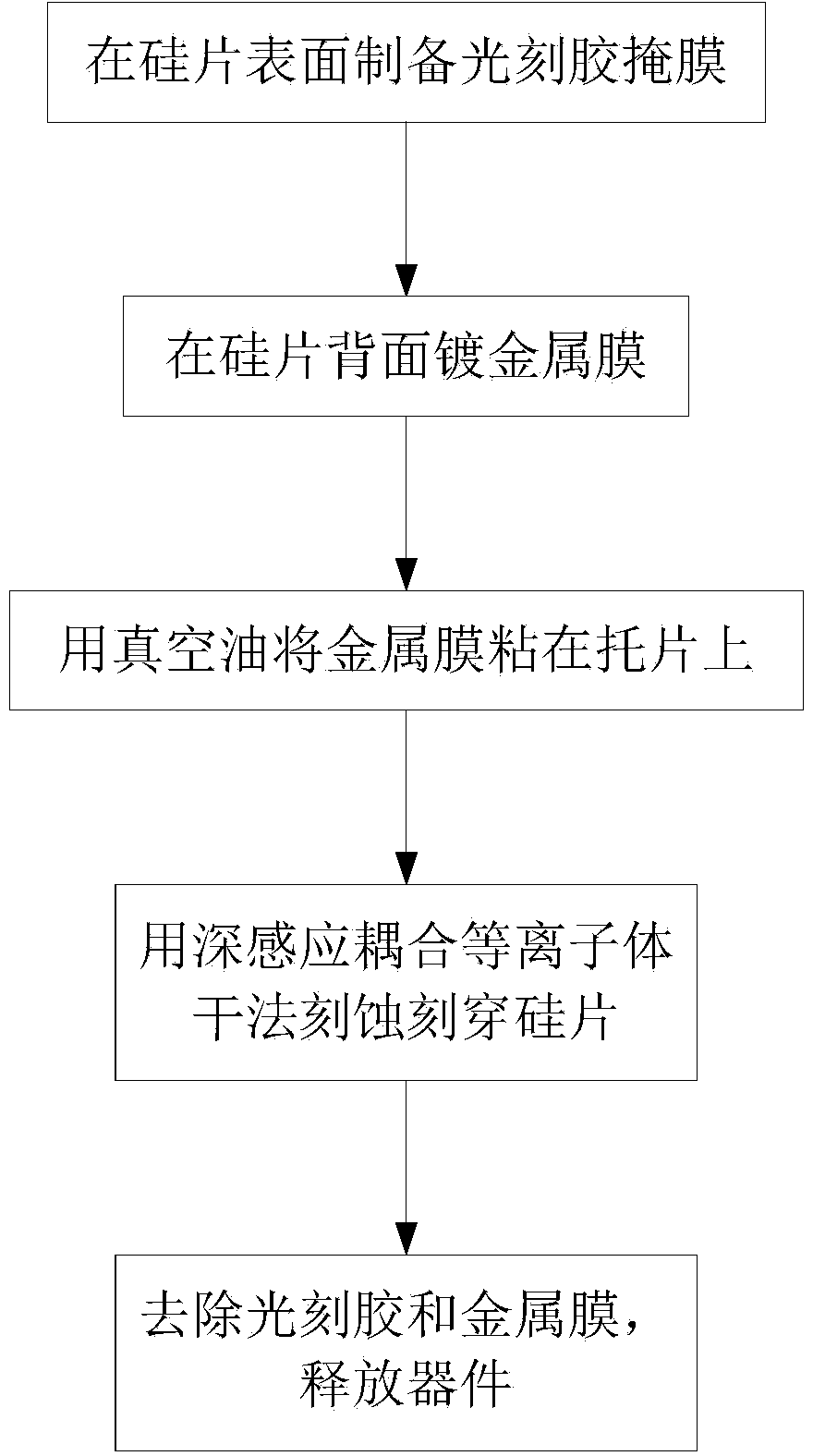
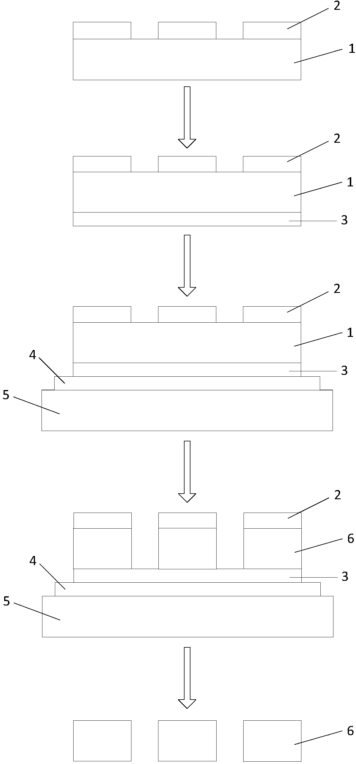
[0045] The bulk silicon processing technology based on silicon waferlithography includes the following steps:
[0046] (1) Design equal etching groove width for the mask pattern of the device to be processed, and prepare a patterned photoresist mask on the surface of the silicon wafer. Further include the following steps:
[0047] (1-1) Carry out organic washing and pickling on the silicon wafer.
[0048] (1-2) After drying the water on the hot plate, evenly distribute the Az9260 photoresist, the rotation speed is 1500r / min, and the thickness of the photoresist is 8μm.
[0075] The bulk silicon processing technology based on silicon wafer lithography includes the following steps:
[0076] (1) Design equal etching groove width for the mask pattern of the device to be processed, and prepare a patterned photoresist mask on the surface of the silicon wafer. Further include the following steps:
[0077] (1-1) Carry out organic washing and pickling on the silicon wafer.
[0078] (1-2) After drying the water on the hot plate, evenly distribute the Az9260 photoresist, the rotation speed is 2500r / min, and the thickness of the photoresist is 5μm.
[0079] (1-3) Pre-bake at 120°C for 3 minutes.
[0080] (1-4) Use a laserdirect writing lithography machine to perform photolithography, equal to the width of the etching groove, such as image 3 Shown, the dose is 2300mj / cm 2 , the defocus amount is -0.006mm.
[0081] (1-5) Develop with a mixture of Az400k developer and ...
PUM
Property
Measurement
Unit
depth
aaaaa
aaaaa
depth
aaaaa
aaaaa
depth
aaaaa
aaaaa
Abstract
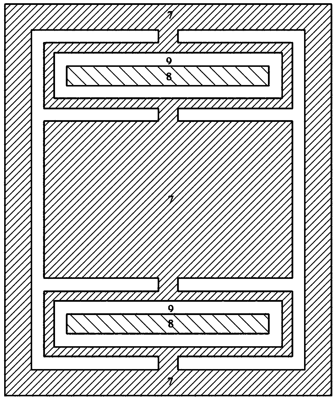
The invention discloses a bulk siliconmachining process based on siliconchipetching and puncturing, which comprises the following steps of preparing a patterned photoresistmask on the surface of a siliconchip; putting a metal film on the back surface of the silicon chip; adhering the metal film to a supporting chip by using vacuum oil, wherein the supporting chip is a silicon chip with an oxide layer on the surface; etching and puncturing the silicon chip to obtain a bulk silicon microstructure by using an inductively coupled plasma dry-etchingsystem, wherein a staged etching method is adopted for inductive coupled plasma dry-etching, and comprises a plurality of etching stages each of which is alternately and cyclically implemented by three steps of passivation, bombardment and etching in an inductive coupled plasmamachine, and along with the increasing of the etching depth, the bombardment intensity of the bombardment step in each etching stage is gradually enhanced; removing the photoresistmask and the metal film, and releasing the bulk silicon microstructure. According to the process, the selection ratio of photoresist, the etching depth and the perpendicularity of the sidewall of an etching groove can be effectively increased.
Description
technical field [0001] The invention belongs to the technical field of microelectronic device processing, and more specifically relates to a bulk silicon processing technology based on silicon slice punching. Background technique [0002] Micro-Electro-Mechanical Systems (MEMS) is a high-tech field developed in recent decades, and MEMS technology based on microelectronic technology has developed particularly rapidly. From the initial surface processing technology to the bulk processing technology, with the development of miniaturization and integration, the deep silicon etching process has become a key process in the manufacturing technology of microelectronic devices. The basic idea of deep silicon etching is the alternating process of reactive ion etching and surface passivation, and the purpose of anisotropic etching is achieved by alternately feeding etching gas and passivating gas. Using this technology can obtain a large aspect ratio and a steep sidewall etching res...
Claims
Application Information
Patent Timeline
Application Date:The date an application was filed.
Publication Date:The date a patent or application was officially published.
First Publication Date:The earliest publication date of a patent with the same application number.
Issue Date:Publication date of the patent grant document.
PCT Entry Date:The Entry date of PCT National Phase.
Estimated Expiry Date:The statutory expiry date of a patent right according to the Patent Law, and it is the longest term of protection that the patent right can achieve without the termination of the patent right due to other reasons(Term extension factor has been taken into account ).
Invalid Date:Actual expiry date is based on effective date or publication date of legal transaction data of invalid patent.

