

Method and apparatus for manufacturing three-dimensional-structure memory device
a memory device and three-dimensional structure technology, applied in solid-state devices, coatings, chemical vapor deposition coatings, etc., can solve the problems of high-capacity data processing and the decrease in the size of the electronic device, and achieve the effect of reducing the volume of the memory devi
- Summary
- Abstract
- Description
- Claims
- Application Information
AI Technical Summary
Benefits of technology
Problems solved by technology
Method used
Image

Examples
Embodiment Construction
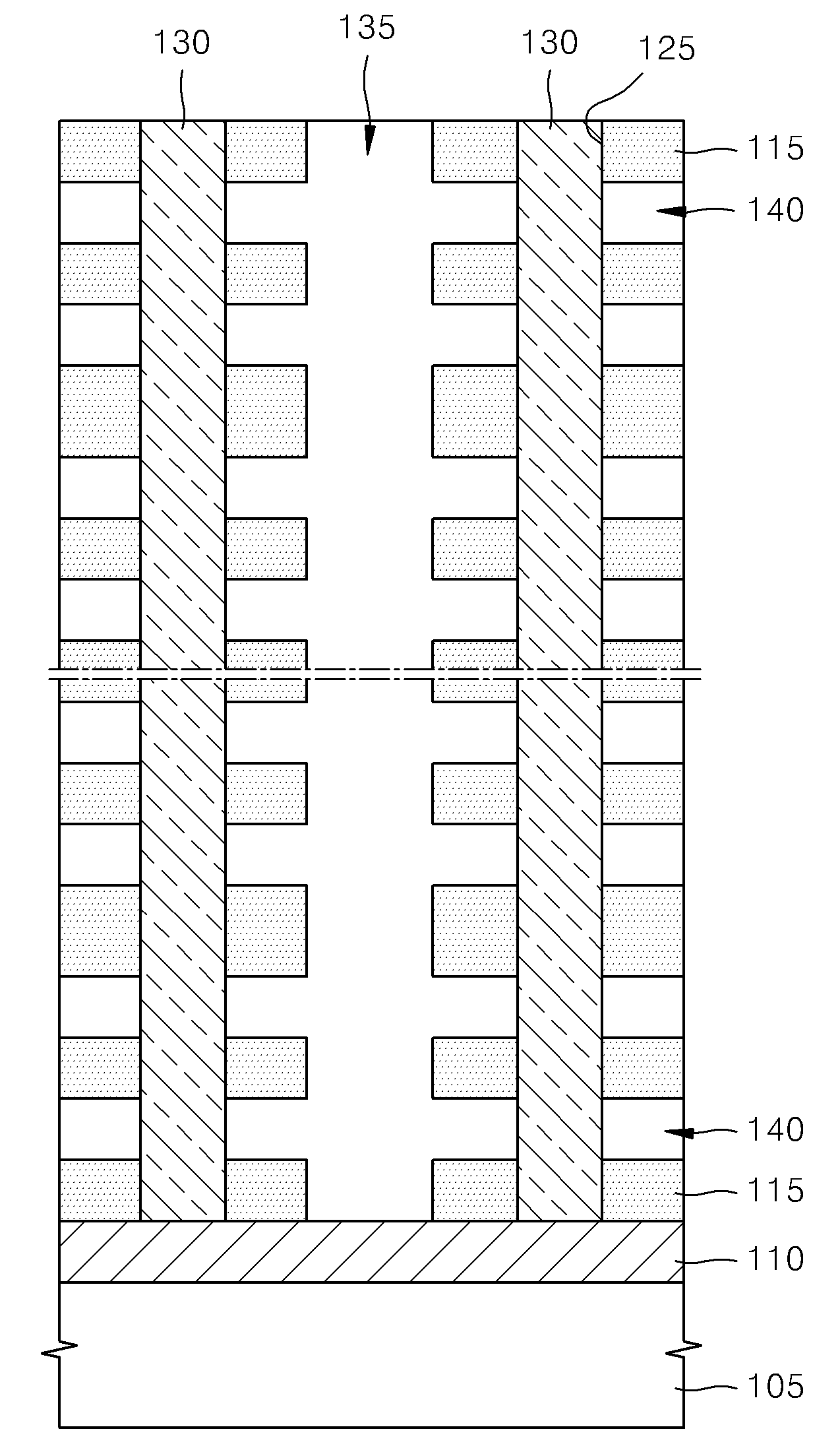
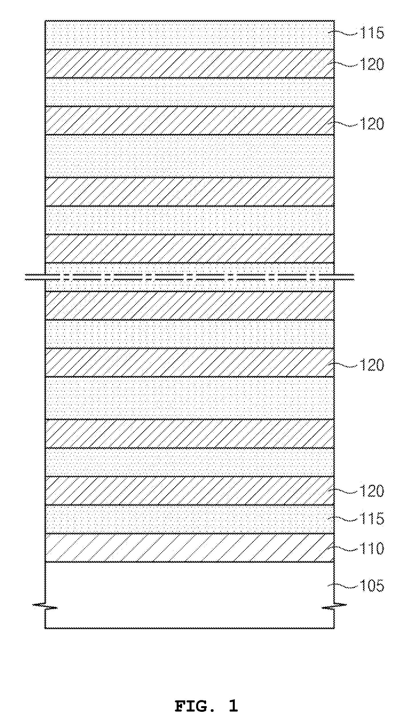
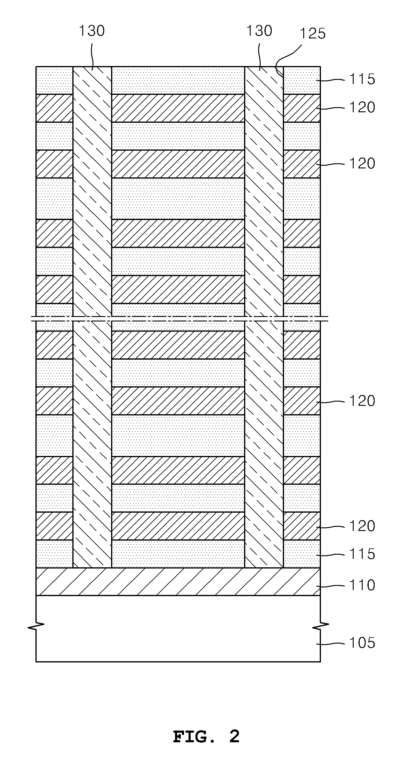
[0027]FIGS. 1 to 6 are schematic cross-sectional views illustrating a method for manufacturing a memory device according to an embodiment of the present invention. Hereinafter, a method for manufacturing a memory device will be described with reference to FIGS. 1 to 6.
[0028]First, as shown in FIG. 1, a substrate 105 may be prepared. The substrate 105 may be formed of a semiconductor material, for example, the group IV semiconductor, the group III-V compound semiconductor, or the group II-VI oxide semiconductor. For example, the group IV semiconductor may include silicon, germanium, or silicon-germanium. The substrate 105 may be provided as a bulk wafer or an epitaxial layer.
[0029]Next, impurities may be injected into an upper portion of the substrate 105 to define an impurity region 110. Then, insulation layers 115 and sacrificial layers 120 may be alternately stacked on the substrate 105. The insulation layers 115 and the sacrificial layers 120 may form an 8×8, 18×18, or n×n multil...
PUM
| Property | Measurement | Unit |
|---|---|---|
| temperature | aaaaa | aaaaa |
| pressure | aaaaa | aaaaa |
| width | aaaaa | aaaaa |
Abstract
Description
Claims
Application Information