Scanning frequency comb microscopy (SFCM) for carrier profiling in semiconductors

a carrier profiling and scanning frequency comb technology, applied in the field of semiconductors, can solve the problems of insufficient measurement average dopant atom concentration for metrology, ssrm is a destructive process, and it is unlikely that much finer resolution can be obtained, so as to achieve non-destructive and refined information for the user

Active Publication Date: 2016-09-13
HAGMANN MARK J
View PDF4 Cites 4 Cited by
  • Summary
  • Abstract
  • Description
  • Claims
  • Application Information

AI Technical Summary

Benefits of technology

[0051]In view of the foregoing disadvantages inherent in the known types of carrier profiling, this invention provides a non-destructive and more precise method by which carrier density may be measured in a semiconductor sample. As such, the present invention's general purpose is to provide a new and improved method that is less complicated than the prior art, non-destructive to the sample, and provides more refined information to the user.

Problems solved by technology

This finer lithography essentially makes a measured average dopant atom concentration insufficient for metrology.
Carrier profiling with a resolution of 1 or 2 nm has been claimed using SSRM but it is unlikely that much finer resolution can be obtained because of the limited strength of materials for the probe tips (L. Zhang, H. Tanimoto, K. Adachi and A. Nishlyama, “l-nm spatial resolution in carrier profiling of ultrashallow junctions by scanning spreading resistance microscopy,” IEEE Electron Device Lett.
Also, SSRM is a destructive process because the surface of the semiconductor is changed by inserting the probe tips, so it is not possible to repeat the measurements at a given location on a sample.
As the inserted probe redistributes sample matter, SSRM is also limited in that adjacent insertion points cannot be so close together as to measure resistance at a disturbed locus (from redistribution) or one where the structural integrity has degraded (from the hole left over from the previous test).
Also, since the probe is inserted into the semiconductor, it cannot be used in a manner to scan the surface of the semiconductor sample as it cannot move seamlessly across that surface.
However, when using SiC or other semiconductors in which the band-gap energy exceeds the photon energy of the laser, there is no frequency comb without a DC tunneling current.
However, with a semiconductor sample the process for dispersal of this charge are more complicated.

Method used


Image

  • Scanning frequency comb microscopy (SFCM) for carrier profiling in semiconductors
  • Scanning frequency comb microscopy (SFCM) for carrier profiling in semiconductors
  • Scanning frequency comb microscopy (SFCM) for carrier profiling in semiconductors

Examples


Embodiment Construction

[0068]With reference now to the drawings, the preferred embodiment of the method of scanning frequency comb microscopy is herein described. It should be noted that the articles “a”, “an”, and “the”, as used in this specification, include plural referents unless the content clearly dictates otherwise.

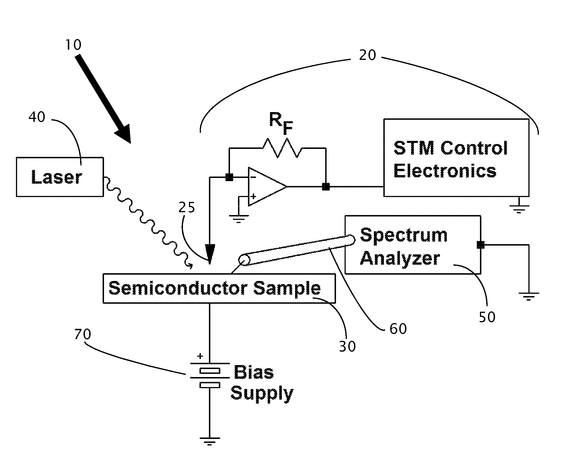
[0069]As can be seen in FIG. 6, in one embodiment, an apparatus set-up 10 is a scanning tunneling microscope 20 positioned over a sample 30 onto which a mode-locked laser 40 is focused so that the laser emits a beam onto the tunneling junction between the STM 20 and the sample 30. The semiconductor sample 30 is forward biased 70, as is shown in FIG. 6 where a p-type semiconductor 30 is used and the voltage on the STM tip 25 is set to make the tip negative, thus allowing the carriers in the semiconductor sample to remain in the region directly beneath the tip. A spectrum analyzer 50 is connected into the circuit by means of a microwave probe 60 making contact with the sample 30 in close p...


PUM

PropertyMeasurementUnit
radiusaaaaaaaaaa
frequenciesaaaaaaaaaa
radiusaaaaaaaaaa

Abstract

A microwave frequency comb (MFC) is produced when a mode-locked ultrafast laser is focused on the tunneling junction of a scanning tunneling microscope (STM). The MFC consists of hundreds of measureable harmonics at integer multiples of the pulse repetition frequency of the laser, which are superimposed on the DC tunneling current. In Scanning Frequency Comb Microscopy (SFCM) the tip and / or sample electrode of the STM is moved vertically and laterally so that the power in the MFC may be measured at one or more locations on the surface of the sample and, from the power, carrier density, and other characteristics, of the sample may be calculated. SFCM is non-destructive of the sample. While many systems are possible to practice SFCM, a preferred apparatus is disclosed.

Description

CROSS-REFERENCES TO RELATED APPLICATIONS[0001]This Application claims priority as a non-provisional perfection of prior filed application No. 61 / 946,403, filed Feb. 28, 2014, and incorporates the same by reference herein in its entirety.FIELD OF THE INVENTION[0002]The present invention relates to the field of semiconductors and more particularly relates to a method by which carrier density may be profiled in a semiconductor using a microwave frequency comb.BACKGROUND OF THE INVENTION[0003]As the semiconductor industry moves from its fifth to sixth decade, the continued advancement in agreement with Moore's Law causes many challenges as the lithography enters the sub-10 nm regime (K. Schuegraf, M. C. Abraham, A. Brand, M. Naik and R. Thakur, “Semiconductor logic technology innovation to achieve sub-10 nm manufacturing,” IEEEJ. Electron Device Soc. 1 (2013) 66-75). One major need, which is listed in the roadmaps for the industry, is new means of metrology to provide much greater resol...

Claims


Application Information

Patent Timeline
Patent Type & Authority Patents(United States)
IPC IPC(8): G01N22/00G01Q60/14G01Q60/10
CPCG01N22/00G01Q60/14
Inventor HAGMANN, MARK J.
Owner HAGMANN MARK J
Why Eureka
Try Eureka