
Solid-state image sensor and camera system

a solid-state image sensor and camera system technology, applied in the field of solid-state image sensors, can solve the problems of deteriorating conversion efficiency, reducing sensitivity during low illumination, and suffering of above-described technologies, so as to suppress deterioration in image quality, increase power consumption, and improve focus detection accuracy during low illumination

Active Publication Date: 2016-09-13
SONY CORP
View PDF25 Cites 2 Cited by
  • Summary
  • Abstract
  • Description
  • Claims
  • Application Information

AI Technical Summary

Benefits of technology

The present technology provides a solid-state image sensor and camera system that can improve focus detection accuracy during low illumination while suppressing deterioration in image quality, yield, increases in power consumption, and costs. This means that the technology can improve focus detection accuracy while reducing power consumption and costs.

Problems solved by technology

However, the above-described technologies suffer from the following drawbacks.
Consequently, conversion efficiency deteriorates, and sensitivity during low illumination decreases, so that low illumination S / N is low.
Consequently, this technology is not suited to pixel miniaturization.

Method used


Image

  • Solid-state image sensor and camera system
  • Solid-state image sensor and camera system
  • Solid-state image sensor and camera system

Examples


first embodiment

2. First Embodiment

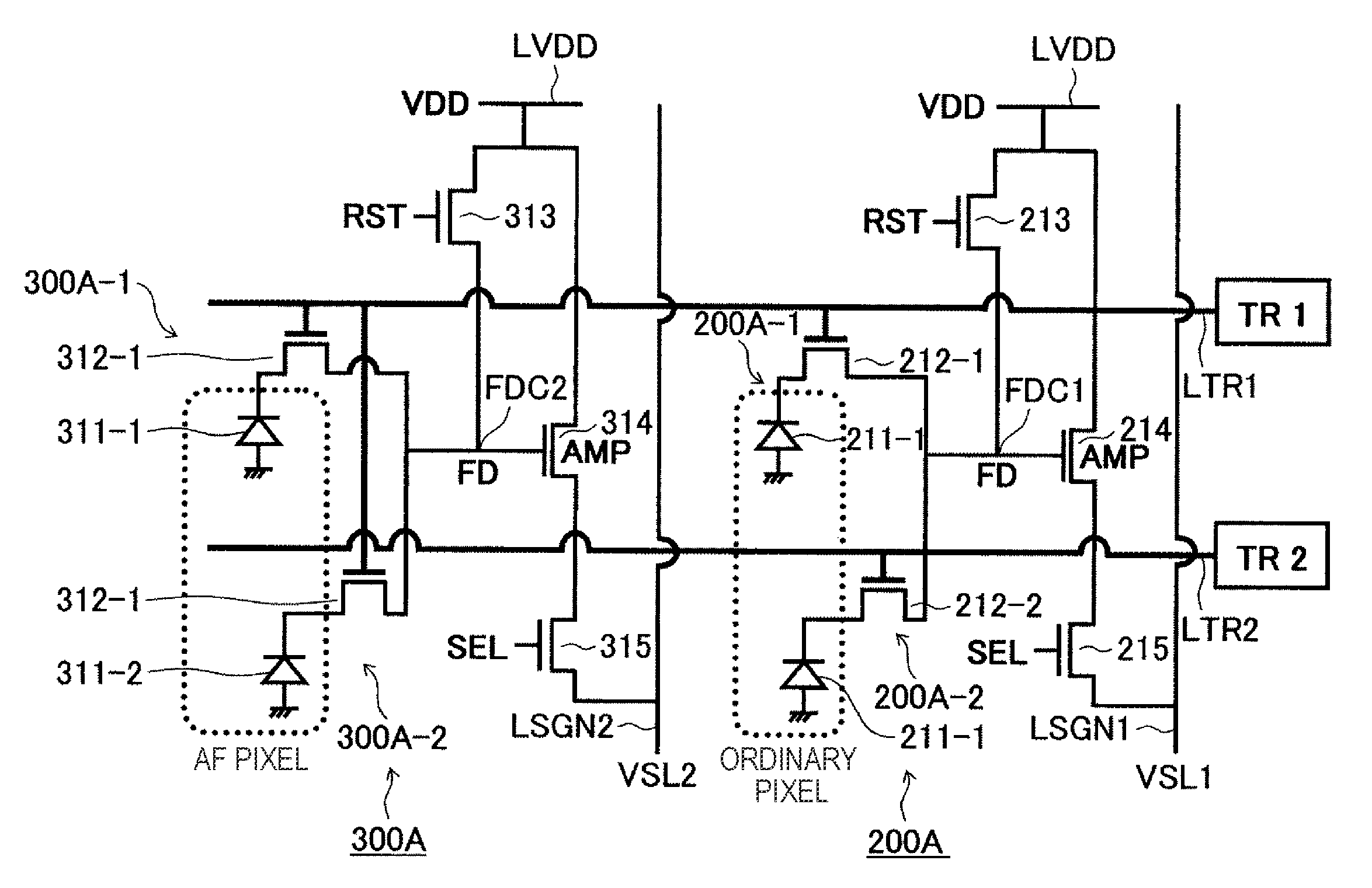
[0188]FIGS. 6(A) and 6(B) are diagrams illustrating a configuration example of vertical 2-pixel-sharing as a first embodiment of the present technology.

[0189]FIG. 6(A) illustrates a vertical 2-pixel-sharing pattern of ordinary imaging pixels, and FIG. 6(B) illustrates a vertical 2-pixel-sharing pattern of focus detection pixels.

[0190]The first embodiment illustrated in FIG. 6 illustrates a configuration of a vertical 2-pixel-sharing pattern that has the same pixel array as described with reference to FIG. 4. For ease of understanding, parts that are the same as in FIG. 4 are represented using the same reference numerals.

[0191]In FIG. 6, the photodiode (PD) photoelectric conversion unit, the floating diffusion layer FD, the gate electrodes, and the transfer control line LTR wires are simply illustrated.

[0192]Further, although for convenience the contacts connecting the FD layers and the wires are not illustrated, in order for the FD portions to be reset, the FD por...

second embodiment

3. Second Embodiment

[0201]FIGS. 7 and 8 are diagrams illustrating a configuration example of a 2-pixel-sharing transfer wire as a second embodiment of the present technology.

[0202]FIG. 7 illustrates a laminate structure of an FD-layer-sharing imaging pixel and focus detection pixel. FIG. 8 schematically illustrates a wire connection in the laminate structure illustrated in FIG. 7.

[0203]Focus detection pixels 300-1 and 300-2 are configured so that photoelectric conversion units PD321 and PD322, transfer gates AFTRG321 and AFTRG322, and a shared floating diffusion layer FD321 are formed on a semiconductor substrate (silicon substrate) 321.

[0204]The transfer gates AFTRG321 and AFTRG322 are raised by a contact CT321 and connected to an intermediate electrode layer 322, which is a first metal layer of an upper layer.

[0205]This intermediate electrode layer 322 is itself raised by a contact CT322 and connected to a transfer control line LTRG1 that is formed from a second metal layer 323 of...

third embodiment

4. Third Embodiment

[0218]FIG. 11 is a diagram illustrating a 4-pixel-sharing pixel array example as a third embodiment of the present technology.

[0219]FIG. 11 illustrates a 2×2-pixel-sharing (4-pixel unit) case.

[0220]Ordinary imaging pixels 200-1 to 200-4, which include photoelectric conversion units PD221 to PD224, are configured so that when a pulse is input in the order of TR1→TR2→TR3→TR4 to the transfer control lines LTR1, LTR2, LTR3, and LTR4, transfer gates TRG1 to TRG4 are turned on / off in order.

[0221]Based on this operation, the signals from the pixels can be read pixel by pixel.

[0222]In the example illustrated in FIG. 11, the focus detection pixels 300-1 to 300-4 are configured so that the transfer gate is connected to only the transfer control line LTR2.

[0223]When a pulse as the transfer control signal TR2 is applied to the transfer control line LTR2, the transfer gates of the four (2×2) focus detection pixels 300-1 to 300-4 are simultaneously turned on, and four pixels wo...


PUM


Abstract

Provided is a solid-state image sensor including a pixel array portion formed from a two-dimensional array of ordinary imaging pixels each having a photoelectric conversion unit and configured to output an electric signal obtained through photoelectric conversion as a pixel signal, and focus detection pixels for detecting focus. The focus detection pixels include at least a first focus detection pixel and a second focus detection pixel each having a photoelectric conversion unit and configured to transfer and output an electric signal obtained through photoelectric conversion to an output node. The first focus detection pixel and the second focus detection pixel share the output node. The first focus detection pixel includes a first photoelectric conversion unit, and a first transfer gate for reading out an electron generated through photoelectric conversion in the first photoelectric conversion unit to the shared output node.

Description

RELATED APPLICATION DATA[0001]This application is a continuation of U.S. patent application Ser. No. 13 / 747,183 filed Jan. 22, 2013, the entirety of which is incorporated herein by reference to the extent permitted by law. The present application claims the benefit of priority to Japanese Patent Application No. JP2012-018383 filed on Jan. 31, 2012 in the Japan Patent Office, the entirety of which is incorporated by reference herein to the extent permitted by law.BACKGROUND[0002]The present technology relates to a solid-state image sensor, represented by a CMOS (complementary metal oxide semiconductor), on which ordinary imaging pixels and focus detection pixels are two-dimensionally arrayed, and a camera system.[0003]An example of a known focus detection technology is pupil division phase difference.[0004]In a pupil division phase difference method, the amount of defocus of an imaging lens is detected by dividing the light beams passing through the imaging lens to form a pair of div...

Claims


Application Information

Patent Timeline
Patent Type & Authority Patents(United States)
IPC IPC(8): H04N5/335H04N5/3745H04N5/369H04N5/378H04N5/374H01L27/146H04N9/04H04N5/232
CPCH04N5/3696H01L27/14607H01L27/14609H01L27/14641H04N5/23212H04N5/374H04N5/37457H04N9/045H01L27/14614H01L27/14643H01L27/14645H04N23/672H04N25/704H04N25/778H04N25/134H04N25/76
Inventor YAMASHITA, KAZUYOSHI
Owner SONY CORP
Learn More