Carrier device, electrical device having a carrier device and method for producing same

a carrier device and carrier technology, applied in the direction of printed circuit assembling, printed circuit non-printed electric component association, printed circuit manufacture, etc., can solve the problems of cte mismatch at least at the interface between the substrate and the mounting area, shifted cte mismatch problem, increased production cost, etc., to reduce the risk of failure and minimize mechanical stress

Active Publication Date: 2016-09-13
OSRAM OLED
View PDF24 Cites 3 Cited by
  • Summary
  • Abstract
  • Description
  • Claims
  • Application Information

AI Technical Summary

Benefits of technology

[0017]For at least some embodiments it can be advantageous if the electrical contact layer is applied with a thickness of greater than or equal to 60 μm. A thickness of greater than or equal to 60 μm and less than or equal to 80 μm has also proved to be particularly suitable.
[0036]In accordance with a further embodiment, an electrical device comprises a carrier device in accordance with the embodiments described above. Furthermore, an electrical component is arranged on the electrical device, said electrical component being electrically and mechanically connected to the at least one ridge-shaped contact region. The electrical and mechanical connection can be formed by a soldering connection, in particular, which can enable a high strength and an efficient heat dissipation from the electrical component to the electrical contact layer. Furthermore, the electrical and mechanical connection can be formed by a sintering connection, which has a low ductility and enables a good thermal linking of the semiconductor chip. In particular, the carrier device for the electrical device can comprise the contact regions described above, such that the further contact region and the ridge-shaped contact region can form two electrical connections for making electrical contact with the electrical component and for mounting said electrical component.
[0037]In accordance with a further embodiment, the electrical component and the carrier device have different coefficients of thermal expansion (CTE). By way of example, the carrier device can be embodied as a printed circuit board, a metal core printed circuit board, a ceramic printed circuit board or an anodically oxidized metal or semimetal foil, for example comprising silicon or aluminum. In the case of a metal core printed circuit board, as carrier, the CTE of the carrier device can substantially correspond to the CTE of the metal core. The carrier device can have, for example, a higher coefficient of thermal expansion than the electrical component. In the case of heating of the carrier device and / or of the electrical component and an unequal thermal expansion thereof associated with said heating, thermomechanical stresses can be compensated for by the mobility of the ridge-shaped contact region on account of the at least one recess or the ridge width of the ridge-shaped contact region which decreases toward the insulating layer. As a result, it is possible to achieve a high reliability of the electrical and mechanical connection of the electrical component to the carrier device, in particular also in the case of cyclic thermomechanical loading. As a result of a preferably large-area further contact region of the electrical contact layer, a good thermal use of the electrical component to the carrier device and thus an effective dissipation of heat from the electrical component can be achieved. Since the CTEs of carrier device and electrical component do not have to be identical in the case of the electrical device described here, cost-effective substrate materials such as metal core printed circuit boards, for example, can be used instead of expensive aluminum nitride ceramic substrates used in the prior art.
[0039]The carrier materials described here can, in particular, also be very robust mechanically, for example in the case of a metal core printed circuit board, for example comprising an aluminum layer as metal core. Mechanical stress concentrations such as can be brought about, for example, by instances of screwing, pinching, bending or similar mechanical loads can then be reduced by a plastic deformation of the carrier device. The risk of a panel fracture is therefore lower by a multiple, compared with a ceramic substrate such as an aluminum nitride ceramic.
[0042]The carrier device described here makes it possible, by means of suitable mechanical structures, in particular the ridge-shaped contact region and the at least one recess in the electrically insulating layer and / or the ridge width of the ridge-shaped contact region which decreases toward the insulating layer, to minimize the mechanical stresses occurring at the interfaces between the carrier device and an electrical component mounted on the carrier device. As a result, it is possible to reduce the risk of failure in the case of thermomechanical loads. As described above, this can be made possible by virtue of the fact that parts of the electrically insulating layer are removed in a targeted manner and / or that the electrical contact layer and in particular the ridge-shaped contact region is slightly etched or undercut in a targeted manner, wherein the ridge-shaped contact region is shaped such that a mechanical elasticity is incorporated and the ridge-shaped contact region is thus embodied in a flexible fashion.

Problems solved by technology

However, this approach has the disadvantage that it is necessary to find suitable substrate materials which have a CTE adapted to the CTE of a semiconductor chip and are electrically insulating and have good thermal conductivity.
However, such a material has the disadvantage that it is very expensive.
If the substrate is furthermore formed with a large area, that is to say has a geometrically larger extent than the semiconductor chip, the CTE mismatch problem is shifted from the interface between the semiconductor chip and the substrate to the interface between the substrate and a mounting area on which the substrate is arranged.
Therefore, the CTE mismatch at least at the interface between the substrate and the mounting area is likewise problematic.
Furthermore, ceramic substrate materials such as, for example, aluminum oxide or aluminum nitride are suitable only to a limited extent for use in relatively large modules.
The low ductility of these materials can result in mechanical problems such as panel fracture, for instance.
As a result of the high costs for example when using aluminum nitride, the production costs are increased and economic viability is thus jeopardized.
In the case of loads arising from thermal cycling, forces which can lead to the failure of the weakest element are built up as a result of this CTE mismatch.
In all these cases, however, the CTEs of semiconductor chip and substrate do not match.
In the case of loading arising from thermal cycling, forces are built up which can lead to damage to the semiconductor chip and / or the interface or connection between the semiconductor chip and the substrate.
As a result, although mechanical forces can be buffered, typical conductive adhesives have a low thermal conductivity of usually approximately 1.8 W / m·K, with the result that the heat loss which can arise during the operation of customary semiconductor chips cannot be effectively dissipated.
However, this does not enable a semiconductor chip to be areally linked to a substrate.
The necessary distance between the solder bumps results in considerable losses in the linking area.
The dissipation of the heat loss by this linking is significantly poorer compared with an areal linking.

Method used


Image

  • Carrier device, electrical device having a carrier device and method for producing same
  • Carrier device, electrical device having a carrier device and method for producing same
  • Carrier device, electrical device having a carrier device and method for producing same

Examples


Embodiment Construction

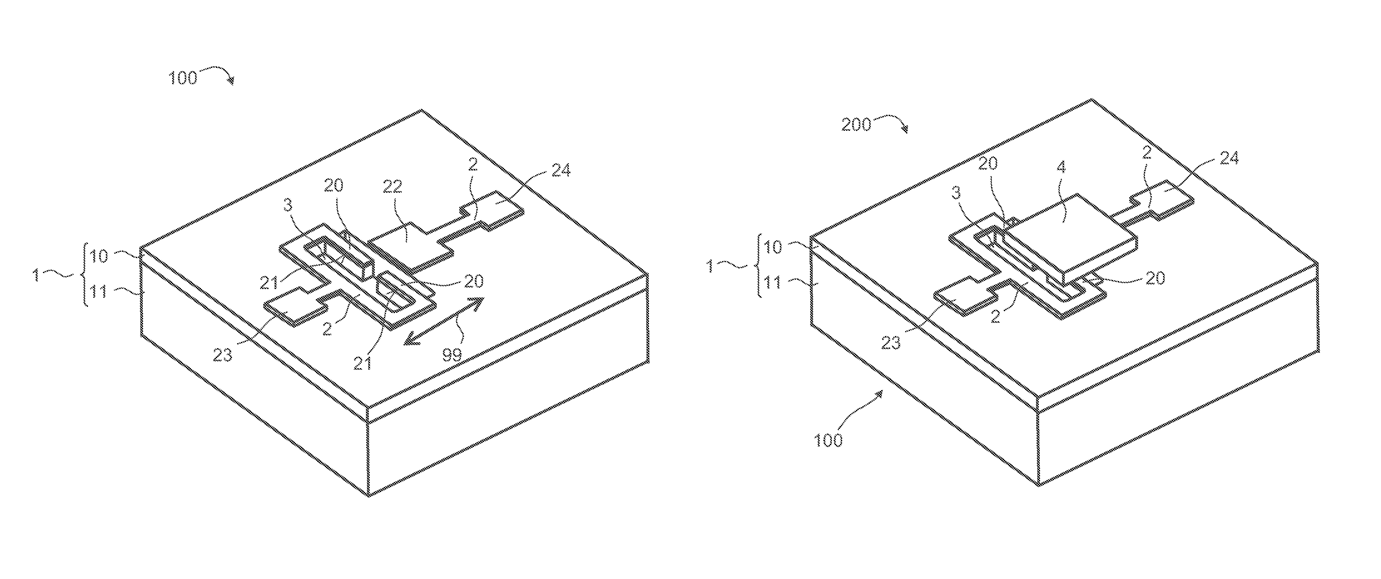
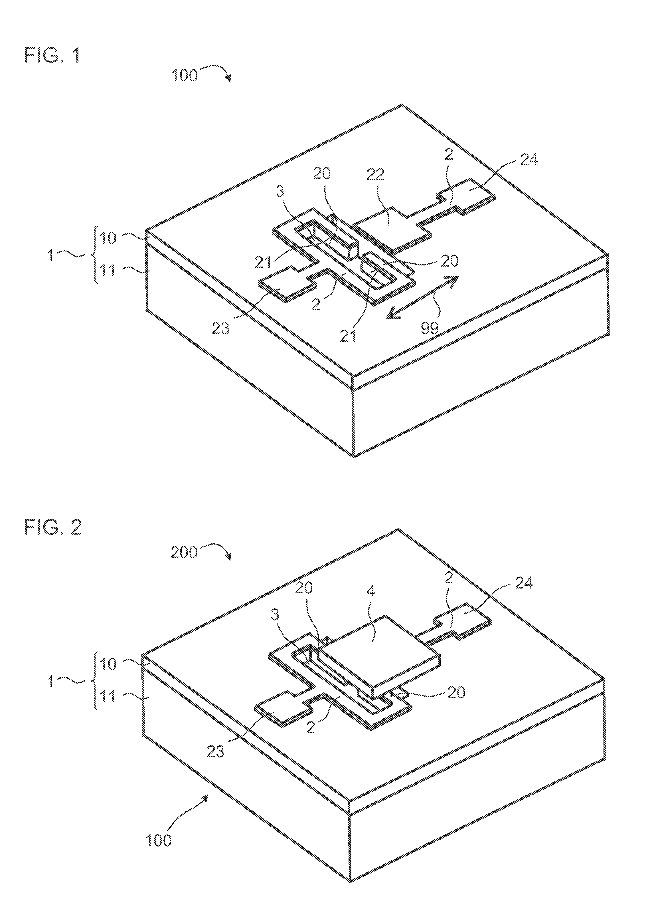
[0049]FIG. 1 shows one exemplary embodiment of a carrier device 100. The carrier device 100 comprises a carrier 1, which, in the exemplary embodiment shown, is formed an electrically insulating layer 10, formed from a plastic material, for example, a plastic material for circuit boards or printed circuit boards, said electrically insulating layer being arranged on a carrier layer composed of a metal, for example, aluminum. By way of example, the electrically insulating layer 10 and the carrier layer 11 can be parts of a metal core printed circuit board (MCPCB), such that the carrier 1 is embodied as a metal core printed circuit board.

[0050]An electrical contact layer 2 is applied on the electrically insulating layer 10, said electrical contact layer forming an interconnection plane of the carrier device 100. As described below in conjunction with a further exemplary embodiment in association with FIGS. 3C and 3D, the electrical contact layer 2 can be produced, for example, by means ...


PUM

PropertyMeasurementUnit
thermal conductivityaaaaaaaaaa
thicknessaaaaaaaaaa
thicknessaaaaaaaaaa

Abstract

A carrier device for an electrical component includes a carrier, which includes an electrically insulating layer, and an electrical contact layer on the electrically insulating layer The electrical contact layer includes at least one bridge-shaped contact region At least one recess in the electrically insulating layer is arranged at least on one side surface of the bridge-shaped contact region and / or the bridge-shaped contact region includes a bridge width reducing toward the insulating layer.

Description

[0001]This patent application is a national phase filing under section 371 of PCT / EP2012 / 063397, filed Jul. 9, 2012, which claims the priority of German patent application 10 2011 079 708.4, filed Jul. 25, 2011, each of which is incorporated herein by reference in its entirety.TECHNICAL FIELD[0002]The present application relates to a carrier device, an electrical device having a carrier device and methods for producing same.BACKGROUND[0003]Semiconductor chips are known whose electrical connections are all arranged on the underside, via which the semiconductor chips are mounted on a substrate. By way of example, light-emitting semiconductor chips are known which can be electrically connected via electrical connection regions on only one side. On account of the customary manner of production and subsequent mounting, which involves applying the connection regions on the top side of semiconductor layer sequences which have already been produced beforehand, said top side then subsequentl...

Claims


Application Information

Patent Timeline
Patent Type & Authority Patents(United States)
IPC IPC(8): H05K1/18H05K3/30H01L33/62
CPCH05K1/183H01L33/62H05K1/18H05K1/182H05K3/301H01L2924/0002Y10T29/49155H01L2924/00
Inventor BERGENEK, KRISTERBIEBERSDORF, ANDREASSORG, JORG ERICH
Owner OSRAM OLED
Why Eureka
Try Eureka