
Imaging apparatus, an electronic device, and imaging method to uniformize distribution of incident light, and a photostimulated luminescence detection scanner

a luminescence detection and imaging method technology, applied in the field of imaging apparatus, can solve the problems of relatively expensive photomultiplier tubes, and achieve the effect of improving the accuracy of photon counting

Active Publication Date: 2016-10-04
SONY SEMICON SOLUTIONS CORP
View PDF7 Cites 3 Cited by
  • Summary
  • Abstract
  • Description
  • Claims
  • Application Information

AI Technical Summary

Benefits of technology

Enhances photon counting accuracy by ensuring uniform light distribution and correcting for high dark current pixels, resulting in improved detection precision and dynamic range.

Problems solved by technology

In such an apparatus, a photomultiplier tube which is relatively expensive is used as a detection unit of weak light.

Method used


Image

  • Imaging apparatus, an electronic device, and imaging method to uniformize distribution of incident light, and a photostimulated luminescence detection scanner
  • Imaging apparatus, an electronic device, and imaging method to uniformize distribution of incident light, and a photostimulated luminescence detection scanner
  • Imaging apparatus, an electronic device, and imaging method to uniformize distribution of incident light, and a photostimulated luminescence detection scanner

Examples


first embodiment

[0050]

[0051][Example of Function Structure of Light Detection Apparatus]

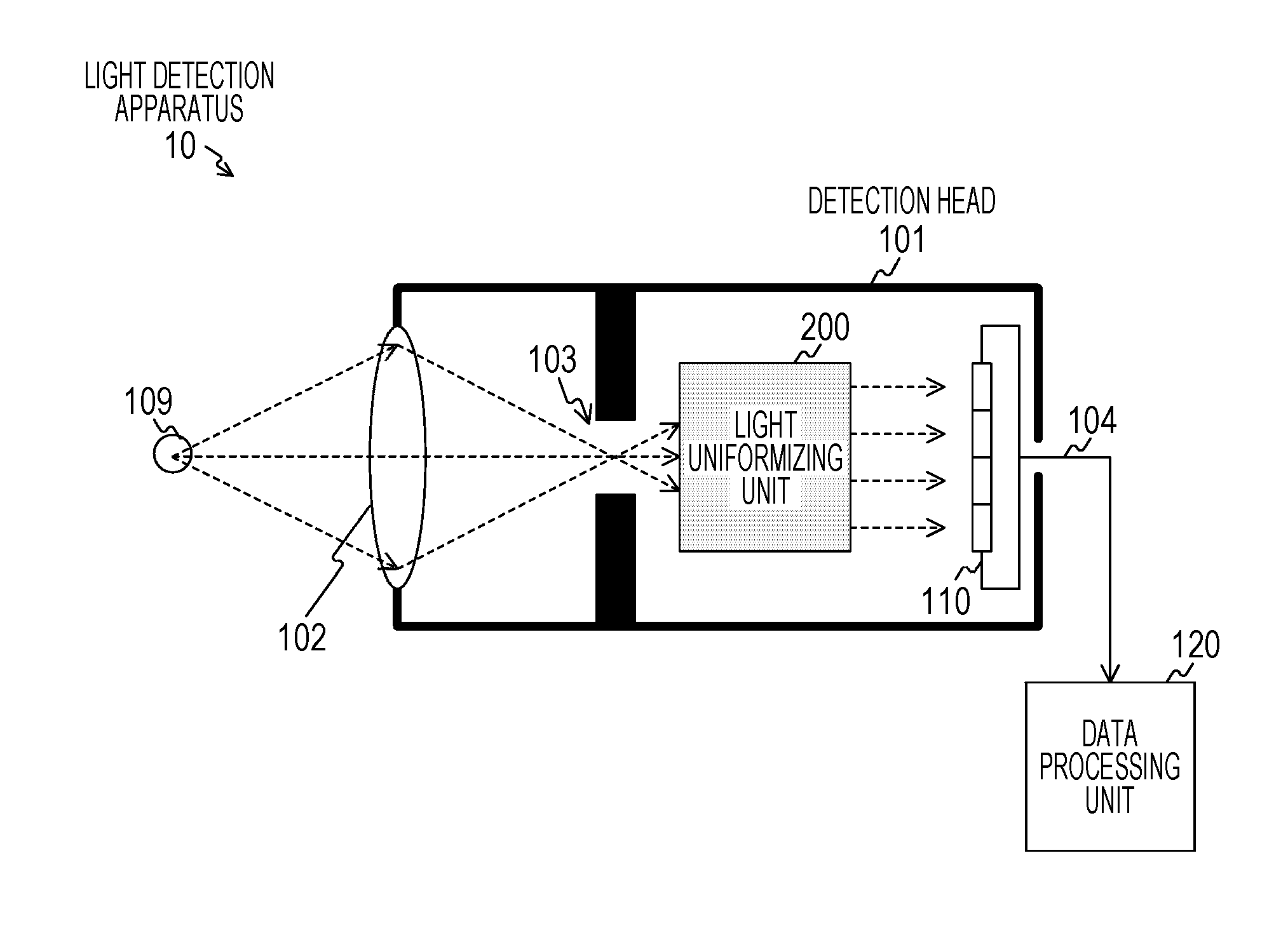
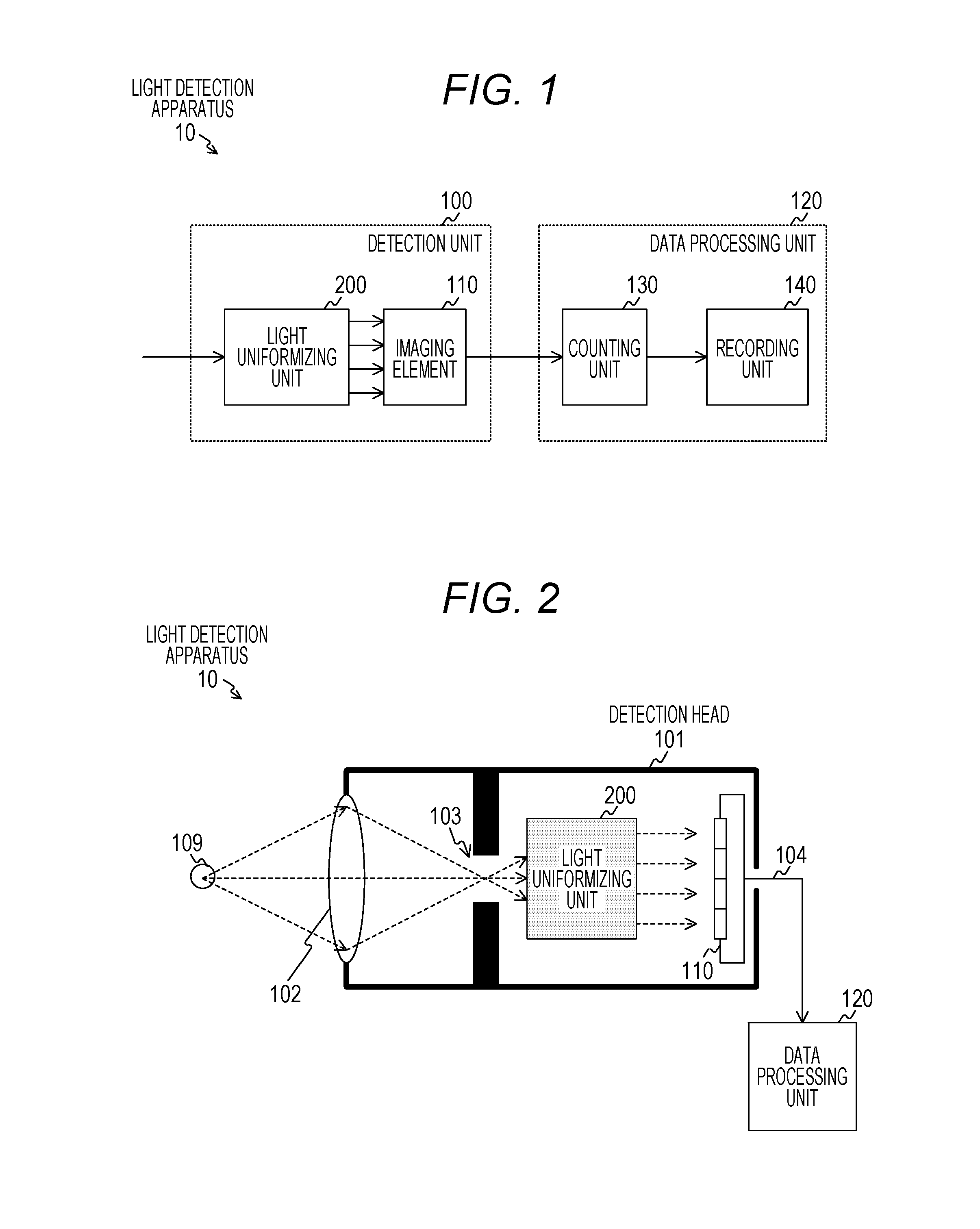
[0052]FIG. 1 is a block diagram illustrating an example of function structure related to a light detection apparatus 10 according to a first embodiment of the present technique.

[0053]The light detection apparatus 10 is an imaging apparatus to perform photon counting by using a complementary metal oxide semiconductor (CMOS) sensor, and includes a detection unit 100 and a data processing unit 120.

[0054]The detection unit 100 converts light incident to the detection unit 100 into a digital signal, and includes a light uniformizing unit 200 and an imaging element 110.

[0055]The light uniformizing unit 200 substantially uniformizes distribution of light (light to be object of photon counting) incident to the detection unit 100, and emits, to a pixel array of the imaging element 110, the substantially uniformized light to be an object of photon counting. That is, the light uniformizing unit 200 distributes light, which...

second embodiment

[0190]

[0191]In the first embodiment of the present technique, the description has been made on the assumption that all of the pixels in the pixel array unit is suitable for photon counting. However, actually, it is difficult to form all of the pixels in a CMOS image sensor as pixels having uniform quality. For example, a pixel having high leakage current (dark current) slightly generated even in a dark state is not suitable for photon counting.

[0192]Thus, in the second embodiment of the present technique, an example, in which count of the pixel having high dark current is made invalid (masked) to improve accuracy of photon counting, will be described with reference to FIG. 10 to FIG. 12.

[0193][Example of Relationship between Size of Dark Current and Number of Pixels]

[0194]FIG. 10 is a view schematically illustrating a relationship between the size of dark current (dark current level) generated in a pixel 310 of the second embodiment of the present technique and the number of the pix...

third embodiment

[0227]

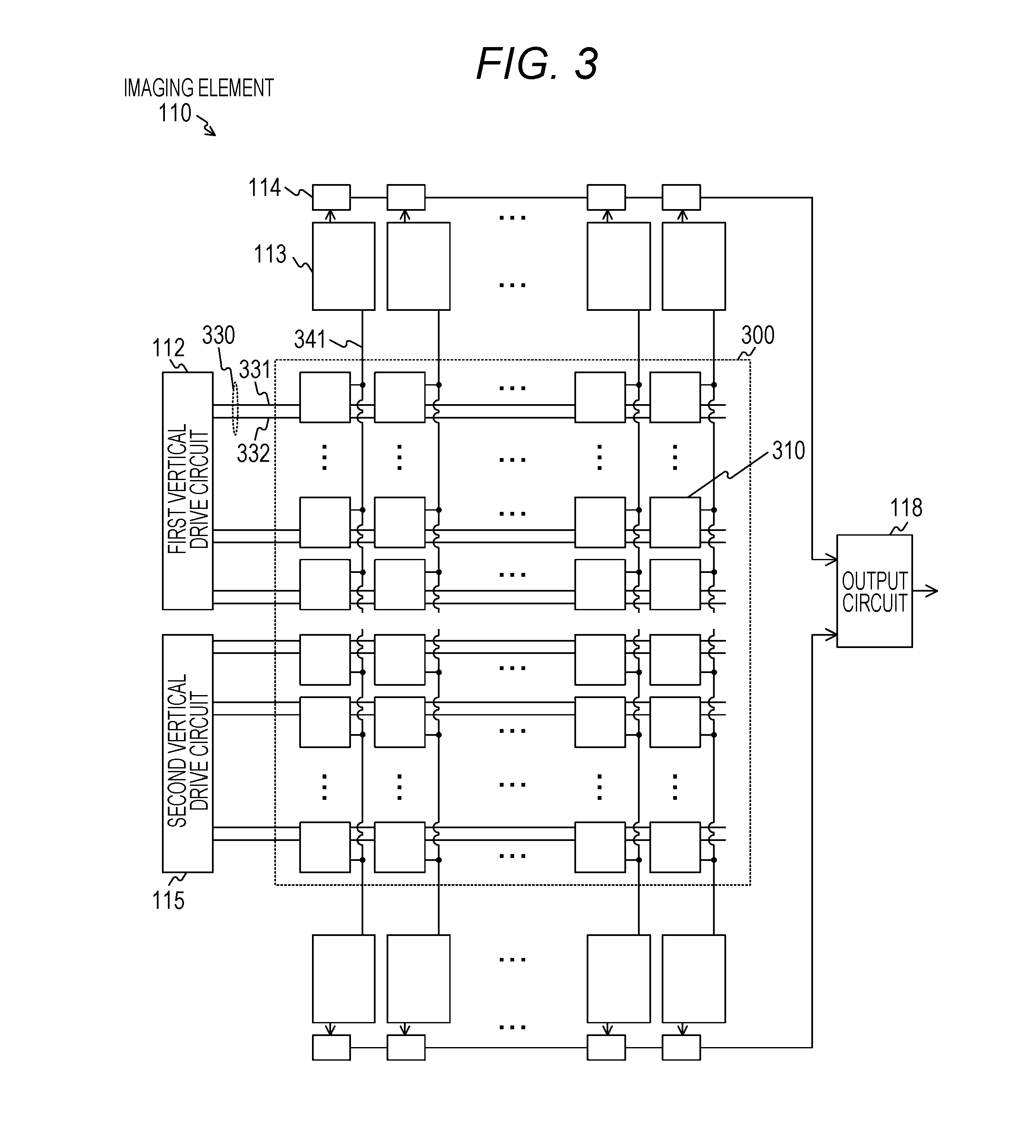
[0228]In the first and second embodiments of the present technique, an example, in which there is one pixel array unit including 128 lines×128 rows of pixels in an imaging element, has been described. An imaging element, which includes such a pixel array unit including small number of pixels, is quite small (for example, 2 mm square). Thus, compared to wafer working process, mounting process may become relatively expensive, in semiconductor manufacturing. Therefore, in an apparatus to which a plurality of detection apparatuses (detection head) is mounted, mounting becomes easy by lining up a plurality of pixel array units, to which a drive circuit and a readout circuit are provided, on the imaging element and by mounting them at once.

[0229]Thus, in the third embodiment of the present technique, an example, in which a plurality of pixel array units is provided on an imaging element, will be described with reference to FIG. 13 to FIG. 15.

[0230][Example of Imaging Element Includi...


PUM

PropertyMeasurementUnit
electric potentialaaaaaaaaaa
timeaaaaaaaaaa
timeaaaaaaaaaa

Abstract

An object is to improve accuracy of photon counting in an imaging apparatus.The imaging apparatus includes a light uniformizing unit. The light uniformizing unit included in the imaging apparatus substantially uniformizes distribution of photons in an orthogonal direction toward an optical axis of incident light, which is incident to an imaging element in the imaging apparatus and the number of photons of which is to be detected, a plurality of pixels being arranged to the imaging element. The light uniformizing unit supplies the uniformized light to the imaging element to which a plurality of pixels are arranged in the imaging apparatus.

Description

TECHNICAL FIELD[0001]The present technique relates to an imaging apparatus. Specifically, the present technique relates to an imaging apparatus including an imaging element to detect weak light, an electronic device including the imaging apparatus, and an imaging method.BACKGROUND ART[0002]Recently, an apparatus to detect weak light has been widely introduced centering on a medical site and a research site. In such an apparatus, a photomultiplier tube which is relatively expensive is used as a detection unit of weak light.[0003]Also, instead of the photomultiplier tube, an apparatus to detect weak light by using a complementary metal oxide semiconductor (CMOS) image sensor, which can be produced at a low price, is proposed (see, for example, Patent Document 1).CITATION LISTPatent Document[0004]Patent Document 1: JP 2011-97581 ASUMMARY OF THE INVENTIONProblems to be Solved by the Invention[0005]In the conventional technique, weak light is detected by counting (photon counting) the nu...

Claims


Application Information

Patent Timeline
Patent Type & Authority Patents(United States)
IPC IPC(8): H01L27/146H04N5/32H04N5/361H04N5/378G01N21/64G01T1/20H04N5/374H04N5/235H04N25/00
CPCH04N5/378H04N5/2351G01N21/645G01T1/2018H01L27/14625H01L27/14658H04N5/2353H04N5/32H04N5/361H04N5/374H01L27/14643H01L27/14627H04N23/73H04N25/63H04N25/70G01T1/20184H04N25/78H04N25/30H04N25/773H04N23/71H04N25/75H04N25/76
Inventor NISHIHARA, TOSHIYUKISUMI, HIROFUMI
Owner SONY SEMICON SOLUTIONS CORP
Learn More