Fine pitch copper pillar package and method

a technology of copper pillars and packages, applied in the field of electronic components, can solve the problems of increasing the diameter of the solder bump, prone to failure, and delicate fine pitch solder bumps, and achieve the effect of maximizing the load bearing area of the copper pillars

Active Publication Date: 2016-10-04
AMKOR TECH SINGAPORE HLDG PTE LTD
View PDF48 Cites 14 Cited by
  • Summary
  • Abstract
  • Description
  • Claims
  • Application Information

AI Technical Summary

Benefits of technology

[0010]By forming the longitudinal length of the copper pillars equal to the length of the bond pad and the latitudinal second width of the copper pillars equal to and aligned with the first latitudinal width of the traces, the load bearing area of the copper pillars on both the bond pads and traces is maximized. By maximizing the load bearing area of the copper pillars, the copper pillars provide robust interconnections that withstand stress due to the differential thermal expansion between the substrate and the electronic component.
[0011]Further, by forming the latitudinal second width of the copper pillars equal to and aligned with the first latitudinal width of the traces, the spacing between adjacent copper pillars and between copper pillars and adjacent traces is equal to the spacing between adjacent traces. Accordingly, the potential for shorting between adjacent copper pillars and between copper pillars and adjacent traces is essentially eliminated.

Problems solved by technology

These fine pitch solder bumps are delicate and prone to failure due to the differential thermal expansion between the substrate and the integrated circuit chip.
More particularly, the load bearing area of the solder bumps is very small and thus the stresses applied thereon are very high due to the thermal expansion mismatch between the integrated circuit chip and the substrate.
However, increasing the diameter of the solder bumps decreases the spacing between adjacent solder bumps and between the solder bumps and adjacent traces.
Accordingly, the potential for shorting between adjacent solder bumps and between solder bumps and adjacent traces increases.

Method used


Image

  • Fine pitch copper pillar package and method
  • Fine pitch copper pillar package and method
  • Fine pitch copper pillar package and method

Examples


Embodiment Construction

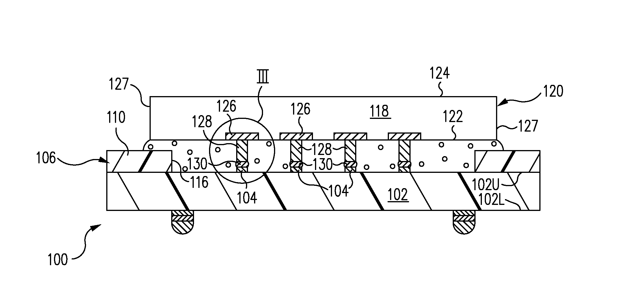
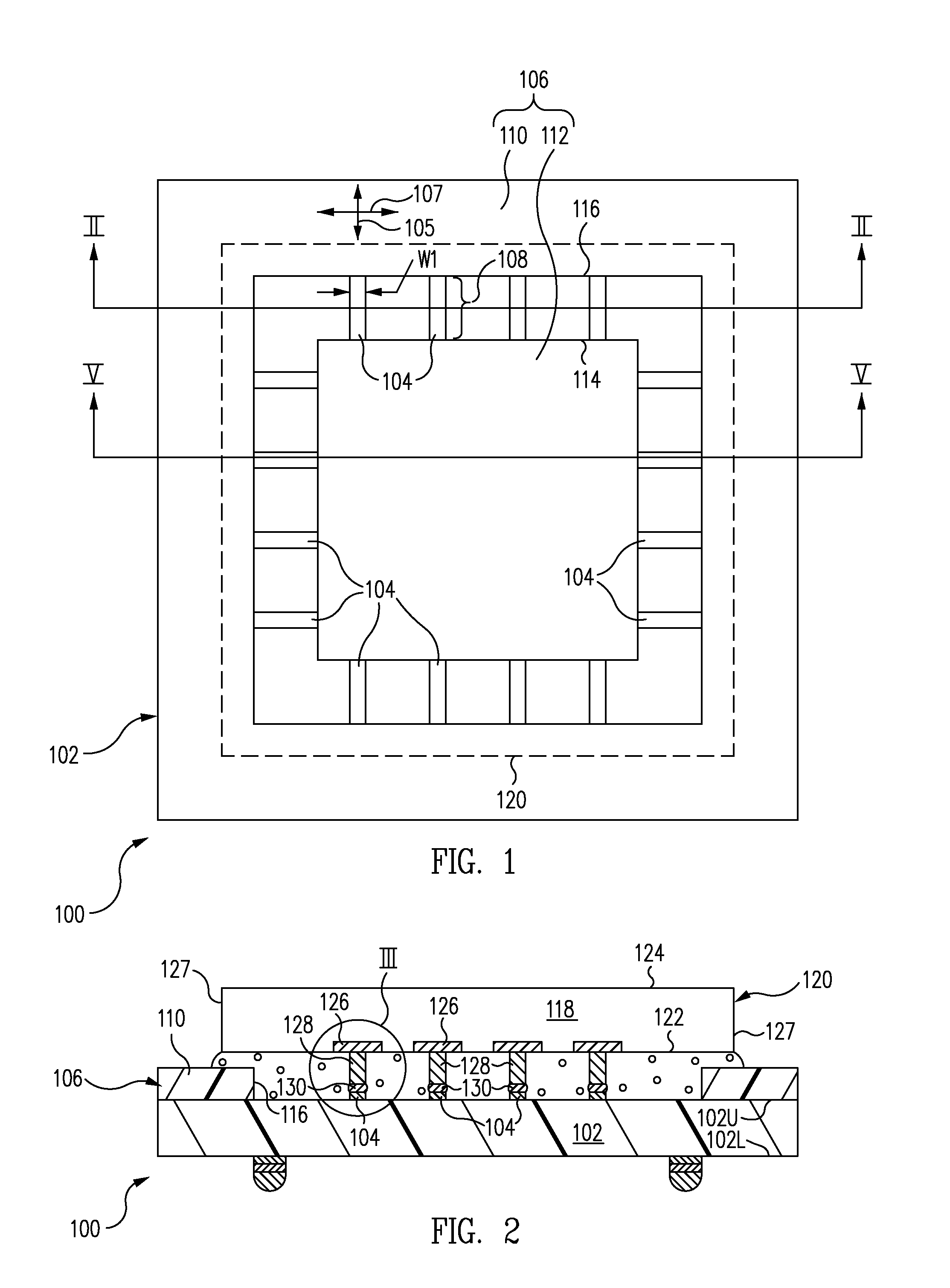
[0024]FIG. 1 is top plan view of a fine pitch copper pillar package 100 in accordance with one embodiment. FIG. 2 is a cross-sectional view of fine pitch copper pillar package 100 along the line II-II of FIG. 1 in accordance with one embodiment.

[0025]Referring now to FIGS. 1 and 2 together, fine pitch copper pillar package 100, sometimes called an electronic component package, includes a substrate 102 including an upper, e.g., first, surface 102U and an opposite lower, e.g., second, surface 102L. Substrate 102 is a dielectric material such as laminate, ceramic, printed circuit board material, or other dielectric material.

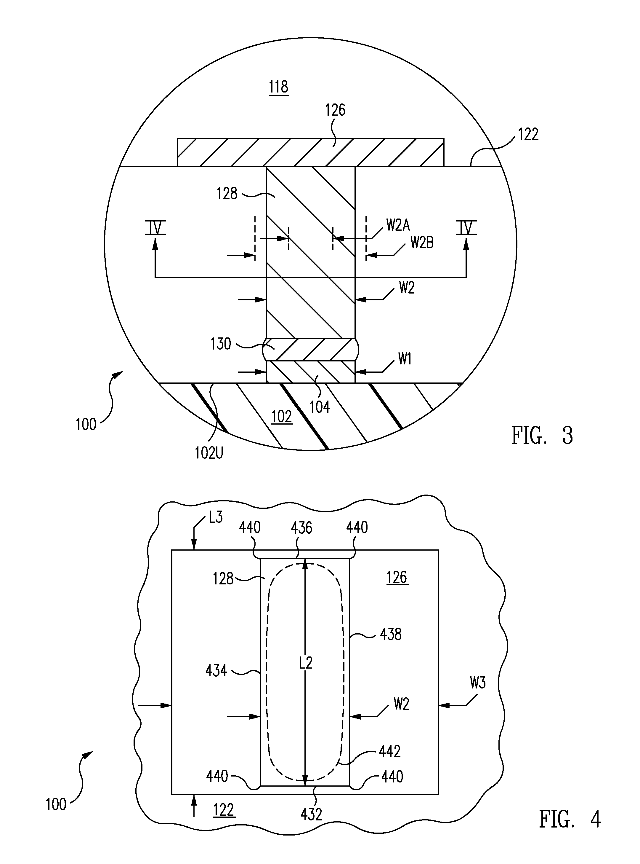
[0026]Formed on upper surface 102U of substrate 102 are electrically conductive upper, e.g., first, traces 104. Also formed on upper surface 102U is a dielectric solder mask 106. Solder mask 106 has formed therein a window 108, sometimes called an opening or a trench in solder mask 106. Portions of upper traces 104 are exposed through window 108 thus facilitating el...


PUM


Abstract

An electronic component package includes a substrate having an upper surface. Traces on the upper surface of the substrate extend in a longitudinal direction. The traces have a first latitudinal width in a latitudinal direction, the latitudinal direction being perpendicular to the longitudinal direction. Rectangular copper pillars are attached to bond pads of an electronic component, the copper pillars having a longitudinal length and a latitudinal second width. The latitudinal second width of the copper pillars is equal to and aligned with the first latitudinal width of the traces. Further, the longitudinal length of the copper pillars is parallel with the longitudinal direction of the trace and equal to the length of the bond pads. The copper pillars are mounted to the traces with solder joints.

Description

RELATED APPLICATIONS[0001]This application is a continuation of Darveaux et al., U.S. patent application Ser. No. 12 / 414,220, filed on Mar. 30, 2009, entitled “Fine Pitch Copper Pillar Package and Method”, which is herein incorporated by reference in its entirety.BACKGROUND OF THE INVENTION[0002]1. Field of the Invention[0003]The present application relates to the field of electronics, and more particularly, to methods of forming electronic component packages and related structures.[0004]2. Description of the Related Art[0005]Fine pitch flip chip technology requires very tight pad to pad spacing on the substrate and very tight bond pad to bond pad spacing on the integrated circuit chip. The pads of the substrate are electrically and physically connected to the bond pads of the integrated circuit chip using fine pitch solder bumps.[0006]These fine pitch solder bumps are delicate and prone to failure due to the differential thermal expansion between the substrate and the integrated ci...

Claims


Application Information

Patent Timeline
Patent Type & Authority Patents(United States)
IPC IPC(8): H05K1/03H05K1/11H05K7/12H05K7/10H05K3/00
CPCH05K1/111H05K3/00H05K3/3436H05K2201/10977H01L24/14H01L2924/15311H01L2224/14133H01L2224/13005H01L24/13H01L24/16H01L2224/02375H01L2224/05541H01L2224/05548H01L2224/05553H01L2224/05554H01L2224/05571H01L2224/1146H01L2224/13007H01L2224/13013H01L2224/13024H01L2224/13082H01L2224/13147H01L2224/1412H01L2224/16237H01L2224/16238H01L2224/26175H01L2224/73204H01L2224/81191H01L2224/81815H01L2224/131H01L23/49894H01L21/563H01L2224/0401H01L2224/16225H01L2224/32225H01L2224/13023H01L23/49838H01L2224/14145H01L2924/00014H01L2924/206H01L2924/00012H01L2924/014H01L2924/00H05K2201/0367H05K2203/0415Y02P70/50
Inventor DARVEAUX, ROBERT FRANCISMCCANN, DAVIDMCCORMICK, JOHNNICHOLLS, LOUIS W.
Owner AMKOR TECH SINGAPORE HLDG PTE LTD
Why Eureka
Try Eureka