Interim oxidation of silsesquioxane dielectric for dual damascene process

a technology of silsesquioxane dielectric and damascene, which is applied in the direction of semiconductor devices, semiconductor/solid-state device details, electrical equipment, etc., can solve the problems of rapid propagation cracks caused by relatively minor physical damage, unprotected ssq materials are not generally considered suitable for layer formation, and most ssq materials are easily attacked

Inactive Publication Date: 2001-11-01
IBM CORP
View PDF0 Cites 2 Cited by
  • Summary
  • Abstract
  • Description
  • Claims
  • Application Information

AI Technical Summary

Benefits of technology

[0014] It is another object of the invention to provide a process by which robust interconnections between devices on a chip can be formed by a dual Damascene process consistent with use of SSQ dielectric materials and high manufacturing yield.
[0016] It is yet another object of the invention to provide protection for a SSQ dielectric material during dual Damascene processing as an incident of other required steps to avoid additional process steps (and variation) and costs associated therewith.

Problems solved by technology

While the dielectric constant is low, the bridging oxygen atoms are strained and can be attacked by numerous chemicals or result in rapidly propagating cracks from relatively minor physical damage.
For that reason, unprotected SSQ materials are not generally considered suitable for formation of layers even though they exhibit good planarizing characteristics that would support high resolution lithographic processes.
However, most SSQ materials are readily attacked by most lithographic resist developers which are generally of high pH.
Moreover, when the SSQ material is attacked by resist developers, the amount of material which may be removed is not readily controllable and may undercut the resist pattern.
Thus, when the SSQ is etched, even with a well-controlled etchant, the resulting via shape may be quite distorted and vias will lack uniformity across the chip and possibly be irregularly and unreliably registered with the structures on the chip to which the vias are to form connections.
Protection of the surface of the SSQ material with a further layer of material such as another dielectric is not practical in some semiconductor structures-such as formation of connection vias in a dual Damascene process.
No technique has been available for avoiding the basic incompatibility of SSQ materials and resist developers in processes requiring a sequence of patterned etch steps, such as in a dual damascene process, particularly for accommodating fine pitch design rules for high density integrated circuits where the low dielectric constant of SSQ materials is particularly critical.

Method used


Image

  • Interim oxidation of silsesquioxane dielectric for dual damascene process
  • Interim oxidation of silsesquioxane dielectric for dual damascene process

Examples


Embodiment Construction

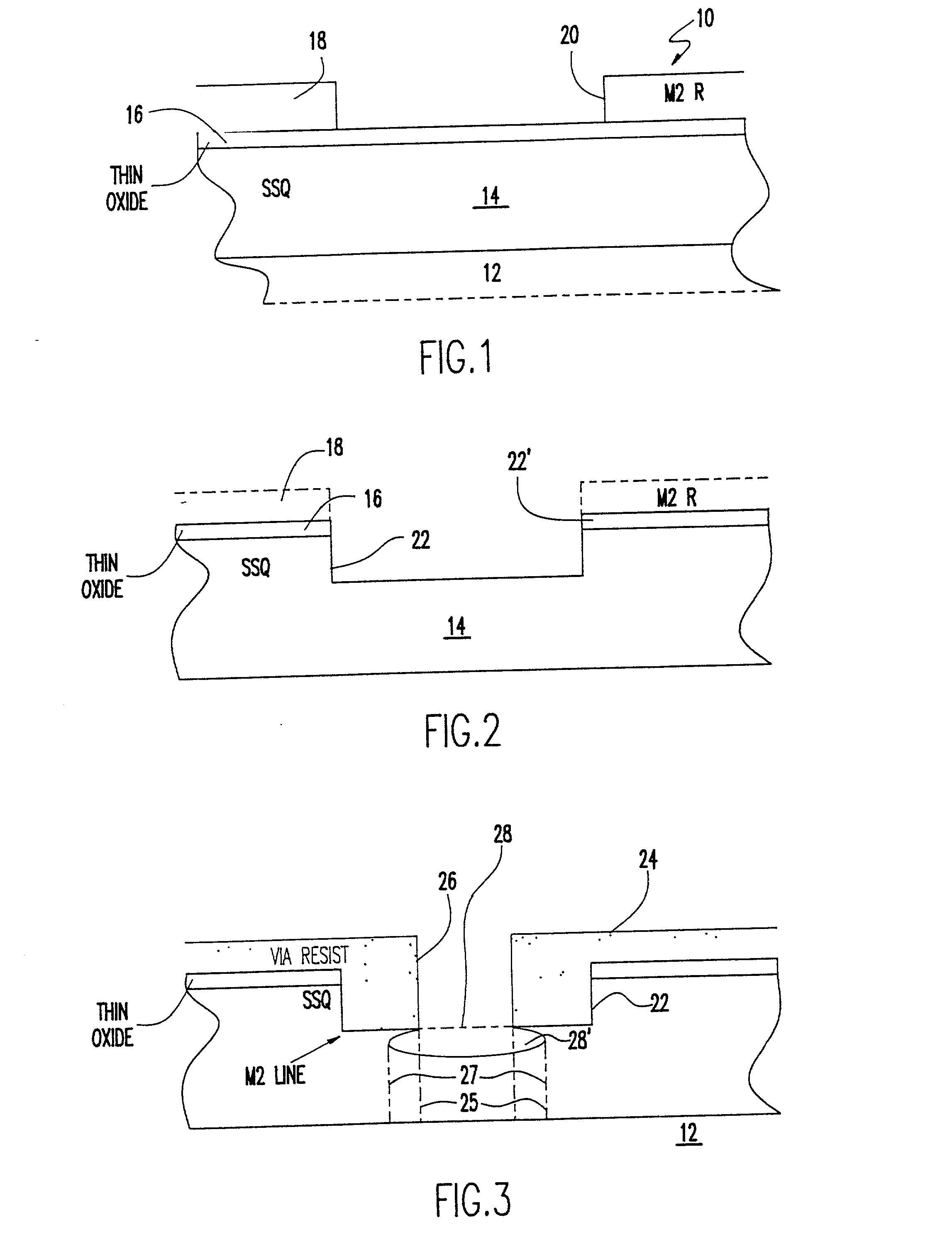
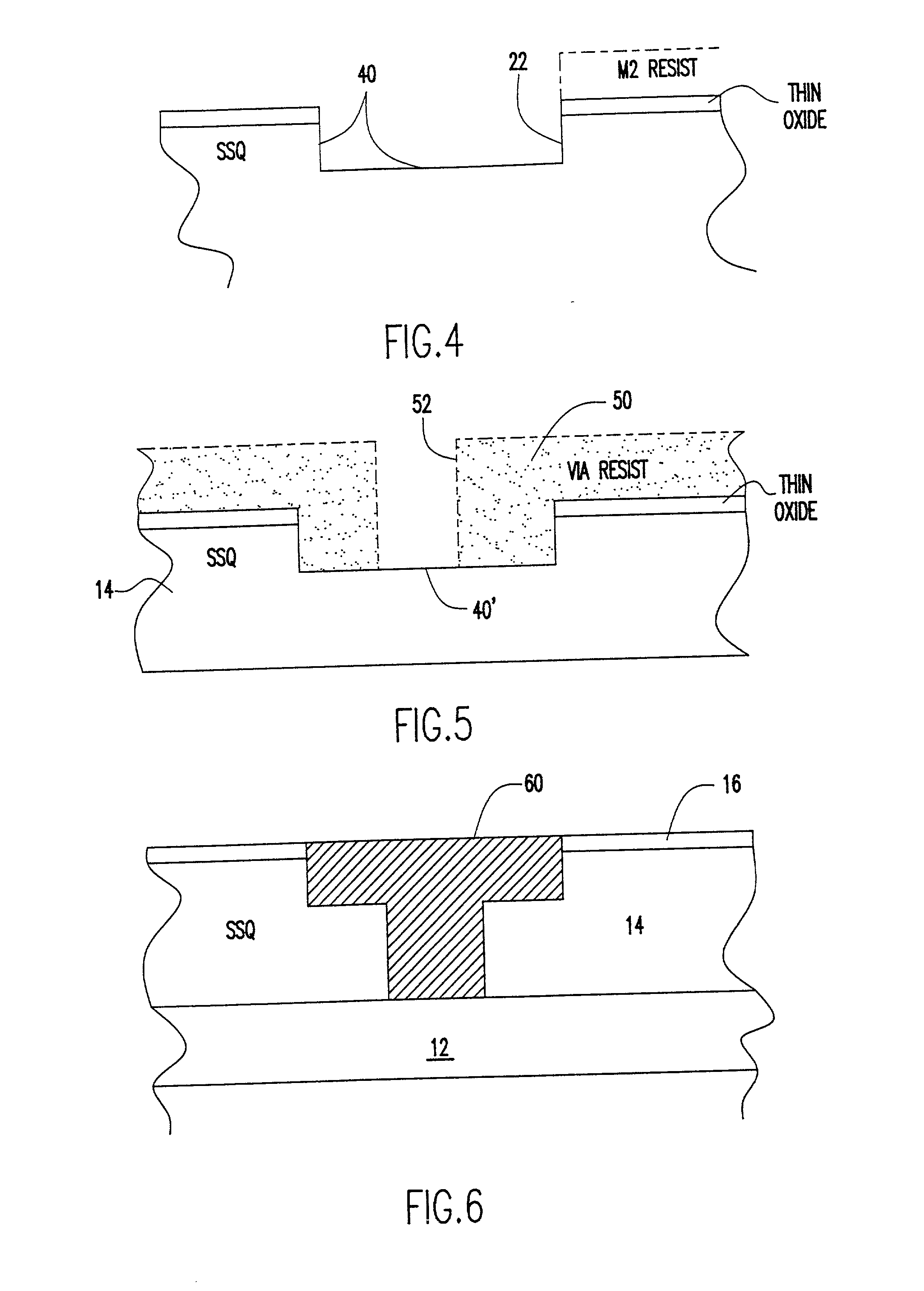
[0024] Referring now to the drawings, and more particularly to FIG. 1, there is shown in cross-section, an early stage in dual Damascene processing to produce conductors at a surface of structure 10 including an integrated circuit chip 12 having devices such as transistors, capacitors and underlying connections (not shown) formed thereon, an SSQ dielectric layer 14, a thin oxide dielectric layer 16 and a patterned resist layer 18. It should be understood that FIGS. 1-3 are not to scale and are disproportionately enlarged in some regions in the interest of clarity. It is also to be understood that while FIGS. 1 and 2 depict early stages of a well-understood dual Damascene process and FIG. 3 is illustrative of the effects of resist development in the absence of the invention, no portion of FIGS. 1-3 is admitted to be prior art as to the present invention.

[0025] The illustration of FIG. 1 assumes prior deposition, processing (e.g. drying), exposure and development of resist layer 18 to...


PUM


Abstract

Resist developers can attack some advanced dielectric materials such as silsesquioxane materials which can be used as an insulator between a surface of an integrated circuit chip and wiring layers formed on the surface of the dielectric material. By performing a resist stripping or etching process in which a reactant material is supplied externally or liberated from the dielectric material, an extremely thin surface protective covering of an intermediate material may be formed which is impervious to resist developers or any of a plurality of other materials which may damage the flowable oxide material. A dual Damascene process for forming robust connections and vias to the chip can thus be made compatible with advanced dielectrics having particularly low dielectric constants to minimize conductor capacitance and support fast signal propagation and noise immunity even where conductors are closely spaced to each other.

Description

[0001] 1. Field of the Invention[0002] The present invention generally relates to integrated circuit manufacturing processes and, more particularly, to processes for forming robust conductive structures on advanced insulating materials.[0003] 2. Description of the Prior Art[0004] Increases in both performance and manufacturing economy with increased integration density have led to the use of design rules with extremely small feature sizes and closeness of spacing in integrated circuit design. Reduced interconnection length between devices included in integrated circuits generally reduces signal propagation time and increases noise immunity. However, as integrated circuits are scaled to smaller design rules, reductions in wiring delays are diminished by increases in resistance (due to decreased cross-sectional area) and capacitance (due to increased connection proximity). This effect can only be ameliorated by reduced resistivity of conductors and / or dielectric constant of insulators...

Claims


Application Information

Patent Timeline
IPC IPC(8): H01L21/28G03F7/40H01L21/302H01L21/3065H01L21/312H01L21/768H01L23/522
CPCH01L21/76808H01L2221/1063H01L21/28
Inventor COOK, ROBERTGRECO, STEPHEN E.HUMMEL, JOHN P.LIU, JOYCEMCGAHAY, VINCENT J.MIH, REBECCASRIVASTAVA, KAMALESH
Owner IBM CORP
Why Eureka
Try Eureka