Method of forming a flexible semiconductor layer and devices on a flexible carrier

Inactive Publication Date: 2016-11-15
ELPIS TECH INC
View PDF12 Cites 6 Cited by
  • Summary
  • Abstract
  • Description
  • Claims
  • Application Information

AI Technical Summary

Benefits of technology

The patent is about a method for making a flexible semiconductor device by removing a portion of the substrate and adding an interfacial release layer to a rigid handle substrate. The method allows for the creation of thin semiconductor devices with improved flexibility. The final step involves removing the substrate from the interfacial release layer using a pressure-sensitive carrier tape or other means. The resulting device can be used for various applications such as flexible displays, sensors, and electronics.

Problems solved by technology

Flexible semiconductor layers produced by spalling techniques (described in U.S. Patent Application Publication No. 2010 / 0311250 A1 to Bedell et al.) can be difficult to process.
The temporary bonding is often incompatible with various processing parameters.
For example, processing of the semiconductor layer / handle substrate assembly may occur at temperatures as high as 180 degrees C. to 250 degrees C. After processing at such temperatures, separation of the semiconductor layer from the handle substrate without causing damage to the semiconductor layer may be difficult.
The difficulty in separation of the semiconductor layer from the handle substrate is generally the result of the temporary bonding utilizing easy-release tapes that are either not stable at the processing temperatures required or which lose their easy-release properties after being exposed to such temperatures.
In addition, air bubbles at the tape / semiconductor layer interface are easy to form yet difficult to remove, the difficulty in removing such bubbles resulting from the tape not being be easily peeled from the semiconductor layer and repositioned without incurring damage.
Difficulty in separation of the semiconductor layer from the handle substrate may also be the result of approaches that utilize epoxies to bond the various layers of the devices.
However, adhesive bonds with epoxies are generally permanent, which thereby inhibits clean separation of the semiconductor layer from the handle substrate.

Method used


Image

  • Method of forming a flexible semiconductor layer and devices on a flexible carrier
  • Method of forming a flexible semiconductor layer and devices on a flexible carrier
  • Method of forming a flexible semiconductor layer and devices on a flexible carrier

Examples


example

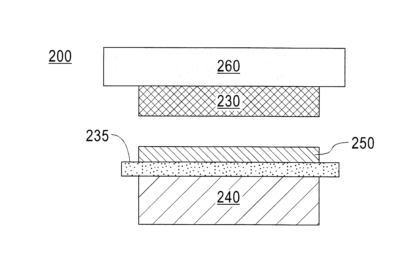
[0079]In one example of a method of using an interfacial release layer as described in FIGS. 2A through 2E, the stressor layer stack 210 was deposited on a 100-oriented silicon (Si) substrate (semiconductor layer 230) to form a silicon film. The stressor layer stack 210 included the adhesion layer 215 of titanium (Ti) (150 nanometers (nm) in thickness) and the seed layer of nickel (Ni) (400 nm in thickness), both deposited by sputtering, and the stressor layer 220 of electroplated Ni (5 micrometers (μm) in thickness) on top of the seed layer of Ni. The Ni was electroplated on a 2 inch diameter area of the Si substrate. The UV releasable tape 225 was then applied to the stressor layer 220 to induce the spelling.

[0080]After the Si film was spelled, a 300 nm aluminum (Al) layer was thermally evaporated on the spelled Si surface without removing the native oxide formed on the Si film after spelling, the Al layer forming the interfacial release layer 250. The Al side of the resulting fle...


PUM


Abstract

A method for fabricating a semiconductor device comprises providing a preformed spalled structure comprising a stressor layer stack on a first surface of a semiconductor substrate; forming an interfacial release layer on an exposed second surface of the semiconductor substrate; adhesively bonding the interfacial release layer to a rigid handle substrate using an epoxy; removing at least a portion of the stressor layer stack from the first surface of the semiconductor substrate; processing the semiconductor substrate; and removing the semiconductor substrate from the interfacial release layer to impart flexibility to the semiconductor substrate.

Description

BACKGROUND[0001]The exemplary embodiments described herein relate generally to semiconductor devices and methods for the fabrication thereof and, more specifically, to methods of using an interfacial release layer to temporarily bond a flexible semiconductor layer to a substrate for the subsequent transfer of the flexible semiconductor layer to a flexible carrier.[0002]Flexible semiconductor layers produced by spalling techniques (described in U.S. Patent Application Publication No. 2010 / 0311250 A1 to Bedell et al.) can be difficult to process. Such techniques generally employ the temporary bonding of a flexible semiconductor layer to a handle substrate and subsequent separation of the flexible semiconductor layer from the handle substrate. The temporary bonding is often incompatible with various processing parameters. For example, processing of the semiconductor layer / handle substrate assembly may occur at temperatures as high as 180 degrees C. to 250 degrees C. After processing at...

Claims


Application Information

Patent Timeline
IPC IPC(8): H01L21/68H01L21/683H01L21/285H01L21/3205H01L21/308H01L21/027H01L23/528H01L21/768
CPCH01L21/6835H01L21/2855H01L21/32051H01L21/308H01L21/0276H01L23/5286H01L21/76877H01L21/76802H01L2221/68381H01L2221/68327H01L2221/68368H01L21/02002H01L2221/68318H01L21/76251H01L21/28568H01L21/32139H01L21/76892H01L23/53209H01L23/53214H01L23/53228H01L23/53242H01L23/53257H01L29/045H01L2221/68359H01L21/4828H01L21/82H01L21/6836H01L21/78
Inventor BEDELL, STEPHEN W.SADANA, DEVENDRA K.SAENGER, KATHERINE L.SALHI, ABDELMAJID
Owner ELPIS TECH INC
Why Eureka
Try Eureka