Techniques for dual dielectric thickness for a nanowire CMOS technology using oxygen growth

a technology which is applied in the field of dual dielectric thickness of nanowires and cmos, can solve the problems of fully depleted technology and no longer an option for doping to adjust v

Inactive Publication Date: 2017-01-03
IBM CORP
View PDF11 Cites 8 Cited by
  • Summary
  • Abstract
  • Description
  • Claims
  • Application Information

AI Technical Summary

Problems solved by technology

Setting multiple Vt's in a fully depleted technology presents many challenges, as doping to adjust Vt is no longer an option.

Method used


Image

  • Techniques for dual dielectric thickness for a nanowire CMOS technology using oxygen growth
  • Techniques for dual dielectric thickness for a nanowire CMOS technology using oxygen growth
  • Techniques for dual dielectric thickness for a nanowire CMOS technology using oxygen growth

Examples


Embodiment Construction

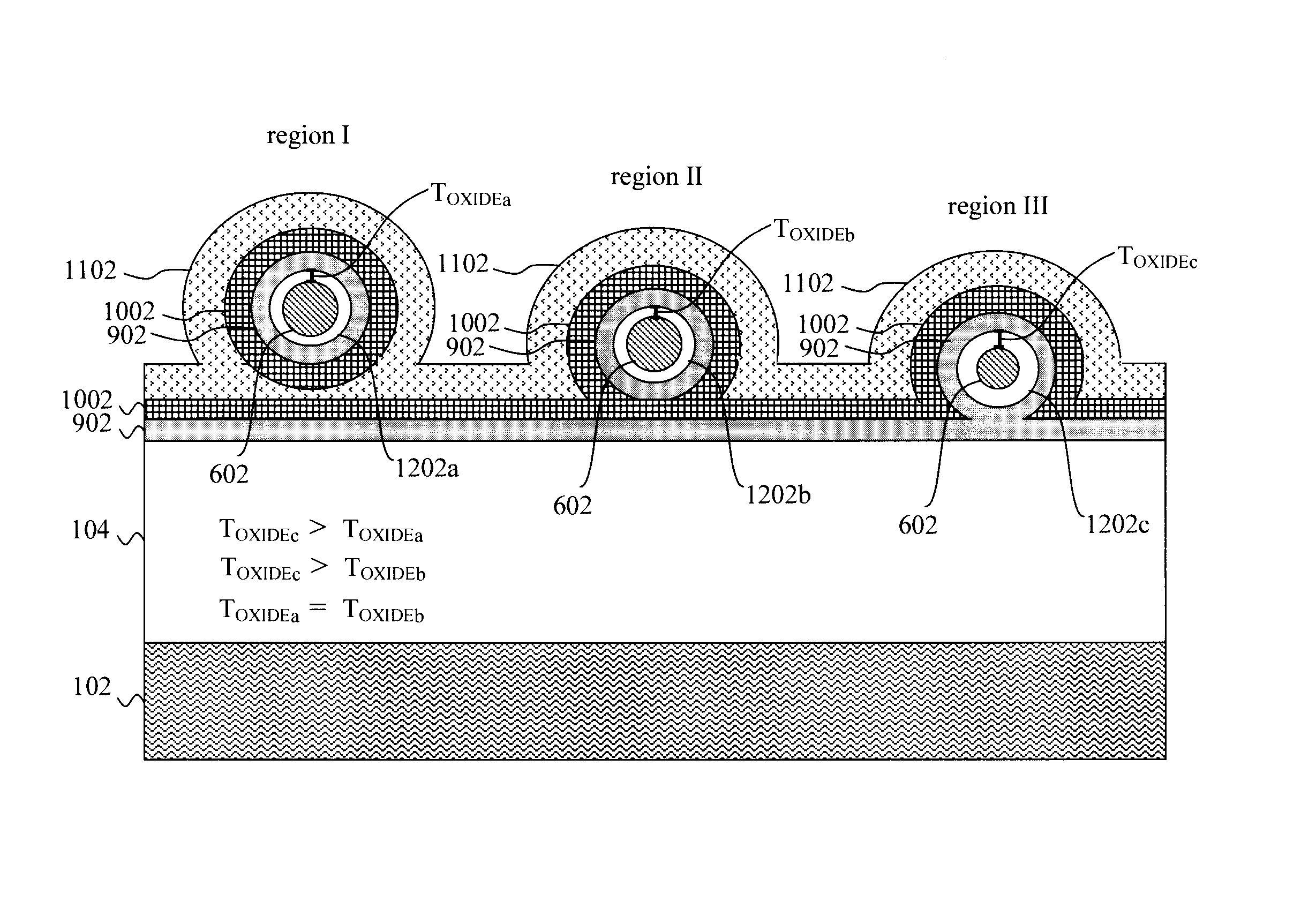
[0033]Provided herein are techniques for controlling the threshold voltage (Vt) of nanowire complementary metal oxide semiconductor (CMOS) devices using a gate first process wherein a suspension height of the nanowires over the buried oxide (BOX) is modulated to control whether or not the high-κ gate dielectric in the present polysilicon / metal / high-κ gate stacks contacts the BOX. The term “high-κ” refers to a material having a dielectric constant κ which is higher than that of silicon (i.e., 11.7). When there is contact between the high-κ gate dielectric and the BOX, a greater amount of oxide growth occurs at the interface between the gate dielectric and the nanowires. Namely, the BOX in that case acts as an additional source of oxygen which diffuses through the high-κ gate dielectric. Oxidation reduces the Vt. See for example, Cartier and U.S. Patent Application Publication Number 2009 / 0289306 A1, the contents of each of which are incorporated by reference as if fully set forth her...


PUM


Abstract

In one aspect, a method of forming a CMOS device includes forming nanowires suspended over a BOX, wherein a first / second one or more of the nanowires are suspended at a first / second suspension height over the BOX, and wherein the first suspension height is greater than the second suspension height; depositing a conformal gate dielectric on the BOX and around the nanowires wherein the conformal gate dielectric deposited on the BOX is i) in a non-contact position with the conformal gate dielectric deposited around the first one or more of the nanowires, and ii) is in direct physical contact with the conformal gate dielectric deposited around the second one or more of the nanowires such that the BOX serves as an oxygen source during growth of a conformal oxide layer at the interface between the conformal gate dielectric and the second one or more of the nanowires.

Description

FIELD OF THE INVENTION[0001]The present invention relates to nanowire complementary metal oxide semiconductor (CMOS) devices and more particularly, to techniques for creating dual dielectric thickness for nanowire CMOS technology using oxygen growth based on varying a suspension height of the nanowires over a buried oxide (BOX).BACKGROUND OF THE INVENTION[0002]Threshold voltage (Vt) is an important parameter to be able to control in metal oxide semiconductor field effect transistor (MOSFET) devices. In bulk MOSFET designs wherein the channel is formed in a bulk semiconductor, the Vt is commonly adjusted through doping. It is often desirable to have multiple Vt's in a MOSFET design wherein the Vt varies from one device to another.[0003]Setting multiple Vt's in a fully depleted technology presents many challenges, as doping to adjust Vt is no longer an option. It has been found that the Vt of planar p-channel FETs can be adjusted through oxidation of the high-κ gate dielectric. See fo...

Claims


Application Information

Patent Timeline
Patent Type & Authority Patents(United States)
IPC IPC(8): H01L27/12H01L27/092H01L21/84H01L21/8238H01L29/423
CPCH01L21/84H01L21/823807H01L27/092H01L27/1203H01L29/42392B82Y10/00B82Y40/00H01L21/823412H01L29/66439H01L29/66772H01L29/775H01L29/78603H01L29/78654H01L29/78696H01L29/1037H01L29/0673H01L2029/42388H01L29/0649
Inventor CHANG, JOSEPHINE B.GUILLORN, MICHAEL A.LAUER, ISAACSLEIGHT, JEFFREY W.
Owner IBM CORP
Why Eureka
Try Eureka