Semiconductor heterostructure with stress management

a heterostructure and stress management technology, applied in the field of semiconductor heterostructures, can solve the problems of high crystal quality growth of group iii nitride devices, difficult growth of sapphire, silicon carbide (sic) and silicon, and low overall efficiency of these devices, so as to reduce internal stresses and reduce the effect of wafer bowing

Active Publication Date: 2017-01-03
SENSOR ELECTRONICS TECH
View PDF9 Cites 7 Cited by
  • Summary
  • Abstract
  • Description
  • Claims
  • Application Information

AI Technical Summary

Benefits of technology

[0009]Aspects of the invention provide a heterostructure for use in fabricating an optoelectronic device. The heterostructure includes a layer, such as an n-type contact or cladding layer, that includes thin sub-layers inserted therein. The thin sub-layers can be spaced throughout the layer and separated by intervening sub-layers fabricated of the material for the layer. The thin sub-layers can have a distinct composition from the intervening sub-layers, which alters stresses present during growth of the heterostructure. The layer can be configured to control stresses present during growth of the heterostructure. To this extent, the thin sub-layers can be configured to reduce internal stresses, wafer bowing, and / or the like.

Problems solved by technology

However, overall efficiencies of these devices remain low.
However, growth of an AlN layer with high crystal quality on substrates formed of sapphire, silicon carbide (SiC) and silicon, which are currently the main substrates for growth of group III nitride devices, is extremely difficult.
While the superlattice approaches allow some control of tensile and compressive stresses in epitaxially grown nitride semiconductor layers, the approaches do not enable epitaxial growth of nitride based semiconductor layers with uniform composition.
While the above approaches work well for epitaxial growth of GaN semiconductor layers, epitaxial growth of aluminum nitride (AlN) layers is more challenging due to a relatively small lateral growth of AlN films.
While the PSS-based approach generally produces an AlN layer with reduced stress and low dislocation densities, the patterning process and subsequent growth of AlN films is technologically complicated and costly.

Method used


Image

  • Semiconductor heterostructure with stress management
  • Semiconductor heterostructure with stress management
  • Semiconductor heterostructure with stress management

Examples


Embodiment Construction

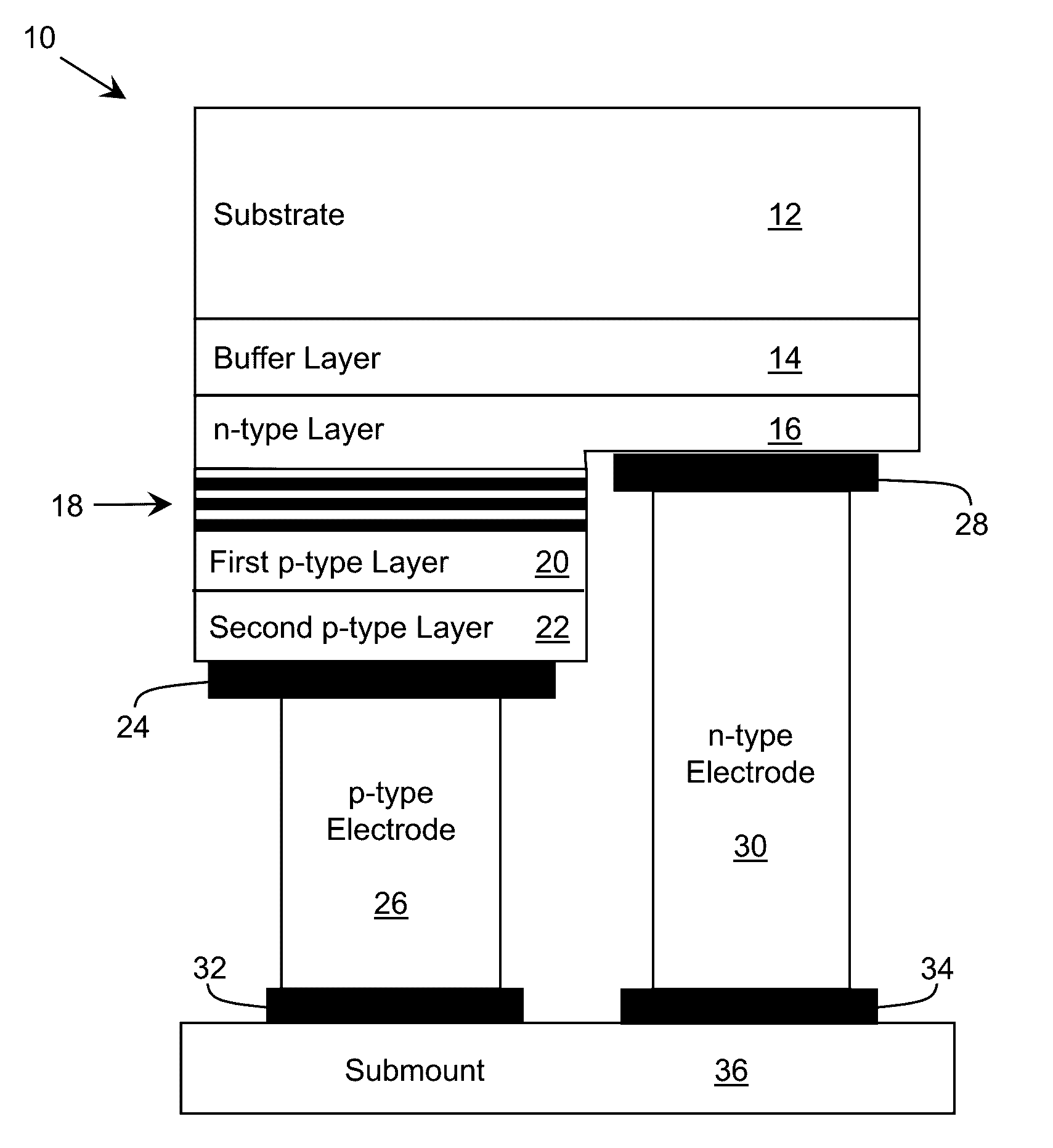
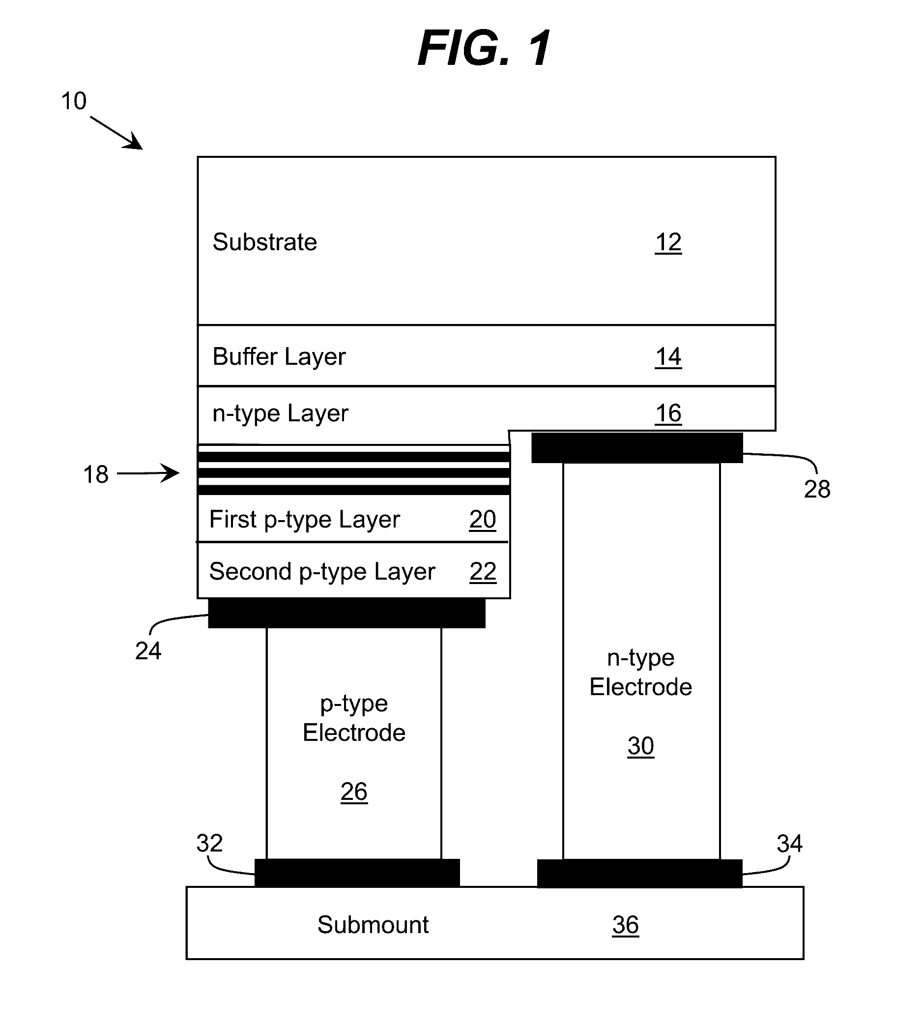
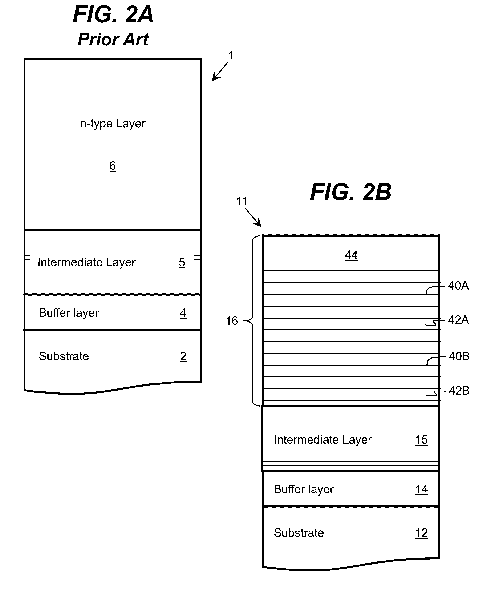
[0027]As indicated above, aspects of the invention provide a heterostructure for use in fabricating an optoelectronic device. The heterostructure includes a layer, such as an n-type contact or cladding layer, that includes thin sub-layers inserted therein. The thin sub-layers can be spaced throughout the layer and separated by intervening sub-layers fabricated of the material for the layer. The thin sub-layers can have a distinct composition from the intervening sub-layers, which alters stresses present during growth of the heterostructure. The layer can be configured to control stresses present during growth of the heterostructure. To this extent, the thin sub-layers can be configured to reduce internal stresses and / or wafer bowing. As used herein, unless otherwise noted, the term “set” means one or more (i.e., at least one) and the phrase “any solution” means any now known or later developed solution.

[0028]The present technique may be combined with the technique of growth of a buf...


PUM

PropertyMeasurementUnit
thicknessaaaaaaaaaa
thicknessaaaaaaaaaa
thicknessaaaaaaaaaa

Abstract

A heterostructure for use in fabricating an optoelectronic device is provided. The heterostructure includes a layer, such as an n-type contact or cladding layer, that includes thin sub-layers inserted therein. The thin sub-layers can be spaced throughout the layer and separated by intervening sub-layers fabricated of the material for the layer. The thin sub-layers can have a distinct composition from the intervening sub-layers, which alters stresses present during growth of the heterostructure.

Description

REFERENCE TO RELATED APPLICATIONS[0001]The current application claims the benefit of U.S. Provisional Application No. 61 / 979,717, which was filed on 15 Apr. 2015, and which is hereby incorporated by reference.TECHNICAL FIELD[0002]The disclosure relates generally to semiconductor structures, and more particularly, to reducing internal stresses and / or wafer bowing during epitaxial growth of semiconductor layers in a semiconductor structure.BACKGROUND ART[0003]Group III nitride semiconductors are widely used for fabricating efficient blue and ultraviolet light emitting devices (e.g., diodes, lasers, etc.), ultraviolet detectors, and field effect transistors. Due to a wide band-gap, these materials are a leading choice for fabricating deep ultraviolet light emitting diodes (DUV LEDs). In recent years, significant advances have been made in improving the efficiency of DUV LEDs. However, overall efficiencies of these devices remain low. For fabrication of DUV LEDs, achieving a high qualit...

Claims


Application Information

Patent Timeline
Patent Type & Authority Patents(United States)
IPC IPC(8): H01L29/06H01L33/24H01L33/20H01L21/02H01L33/00H01L33/32H01L29/15H01L29/20
CPCH01L33/32H01L21/0254H01L21/02458H01L21/02507H01L33/007H01L33/0075H01L33/20H01L33/24H01L29/155H01L29/2003H01L2224/16225H01L33/0062H01L33/12H01L33/30H01L33/0025H01L33/06
Inventor BILLINGSLEY, DANIEL D.KENNEDY, ROBERT M.SUN, WENHONGJAIN, RAKESHSHATALOV, MAXIM S.DOBRINSKY, ALEXANDERSHUR, MICHAELGASKA, REMIGIJUS
Owner SENSOR ELECTRONICS TECH
Why Eureka
Try Eureka