Write assist circuit integrated with leakage reduction circuit of a static random access memory for increasing the low voltage supply during write operations

a static random access memory and leakage reduction technology, applied in static storage, information storage, digital storage, etc., can solve the problems of increasing the dynamic power consumption of the sram circuit and the increase of the circuit area, so as to reduce the leakage

Active Publication Date: 2017-01-10
SYNOPSYS INC
View PDF5 Cites 10 Cited by
  • Summary
  • Abstract
  • Description
  • Claims
  • Application Information

AI Technical Summary

Benefits of technology

[0005]Embodiments relate to circuits for operating an SRAM. The circuit comprises a bias transistor and a write assist circuit. The bias transistor has a first terminal, a second terminal, and an input terminal. The first terminal of the bias transistor is connected to a voltage supply line of SRAM cells. The second terminal of the bias transistor is connected to a first reference voltage. The input terminal of the bias transistor receives a first input voltage that turns the bias transistor on to maintain the voltage supply line at a first voltage level. The input terminal of the bias transistor also receives a power save signal during a power save operation of the SRAM cells. The power save signal turns the bias transistor on to maintain the voltage supply line at a second voltage level higher than the first voltage level during a power save mode of a device using the SRAM. Maintaining the voltage supply at the second voltage level reduces leakage through the supply line during the power save mode. The input terminal of the bias transistor receives a write assist pulse during a write operation of the SRAM cells. The write assist pulse causes the bias transistor to turn off, thereby disconnecting the voltage supply line from the first reference voltage. The write assist circuit has an input terminal connected to the input terminal of the bias transistor and an output terminal connected to the voltage supply line. The input terminal of the write assist circuit receives the write assist pulse. Responsive to the write assist pulse, the write assist circuit increases the voltage of the voltage supply line to a third voltage level higher than the first voltage level. Increasing the voltage of the voltage supply line to the third voltage level during a write operations assists the SRAM with the write operation. The reuse of the bias transistor for power save mode and for the write assist operation provides savings in the area of the write assist circuit.

Problems solved by technology

These write assist schemes often result in increase in dynamic power consumption of the SRAM circuits and also increase area of the circuit.

Method used


Image

  • Write assist circuit integrated with leakage reduction circuit of a static random access memory for increasing the low voltage supply during write operations
  • Write assist circuit integrated with leakage reduction circuit of a static random access memory for increasing the low voltage supply during write operations
  • Write assist circuit integrated with leakage reduction circuit of a static random access memory for increasing the low voltage supply during write operations

Examples


Embodiment Construction

[0022]The Figures (FIG.) and the following description relate to preferred embodiments by way of illustration only. It should be noted that from the following discussion, alternative embodiments of the structures and methods disclosed herein will be readily recognized as viable alternatives that may be employed without departing from the principles of the embodiments.

[0023]Reference will now be made in detail to several embodiments, examples of which are illustrated in the accompanying figures. It is noted that wherever practicable, similar or like reference numbers may be used in the figures and may indicate similar or like functionality. The figures depict embodiments for purposes of illustration only.

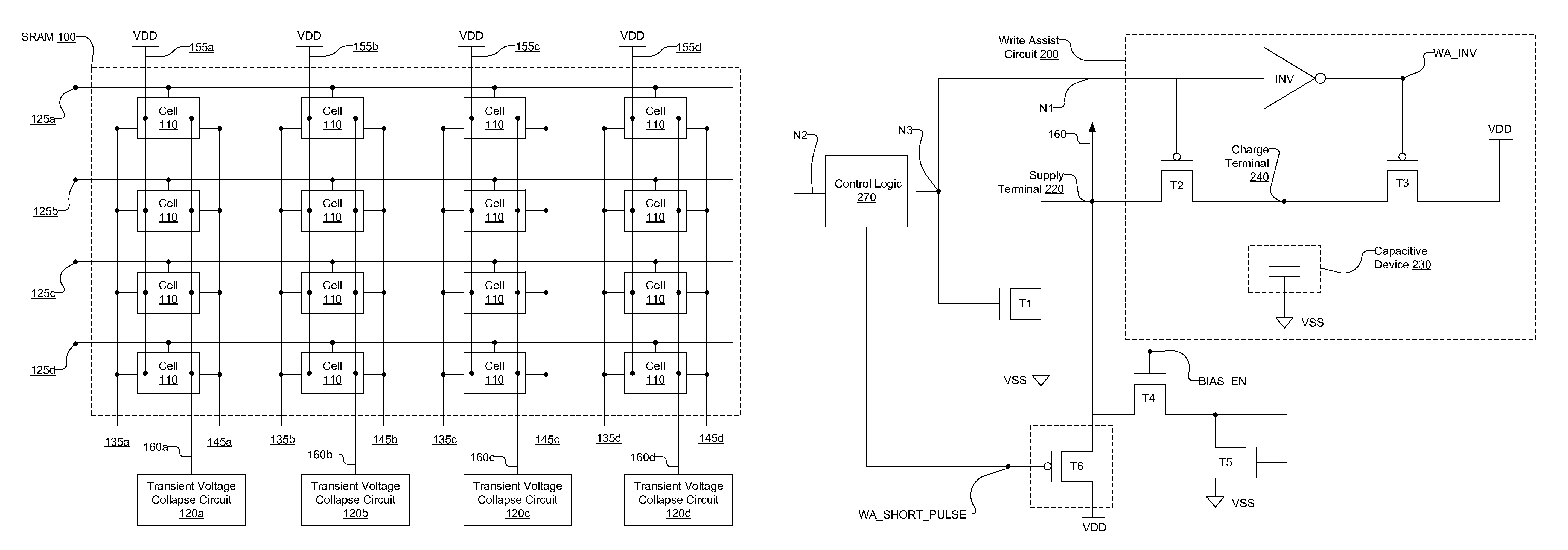
[0024]FIG. 1 shows an SRAM circuit receiving voltage supply from a transient voltage collapse circuit, according to an embodiment. A letter after a reference numeral, such as “125a,” indicates that the text refers specifically to the element having that particular reference numeral. ...


PUM


Abstract

A transient voltage collapse circuit provides a reference voltage for an SRAM (static random access memory). The SRAM receives a first reference voltage and a second reference voltage higher than the first reference voltage. The transient voltage collapse circuit provides the first reference voltage to the SRAM via a voltage supply line. The transient voltage collapse circuit maintains the voltage supply line at a first voltage level during a power save mode of the SRAM. The transient voltage collapse circuit increases the voltage of the voltage supply line during a write operation of the SRAM. The increase in the voltage of the supply line reduces the gap between first reference voltage and the second reference voltage, thereby assisting with the write operation of the SRAM.

Description

BACKGROUND[0001]1. Field of the Disclosure[0002]The present disclosure relates to static random access memory (SRAM) circuits in general and in particular to low power write assist techniques for SRAM circuits.[0003]2. Description of the Related Art[0004]Static random access memory (SRAM) is often included in very large scale integration VLSI system-on-chip (SoC) applications. The size of the SRAM circuit has a significant impact on the overall size of an integrated circuit for such applications. Therefore, there is a need to keep the size of SRAM circuits small. Furthermore, there is a trend towards reducing operation supply voltage of these integrated circuits. Reliability of the SRAM circuits reduces as supply voltages are reduced due to variations in circuit characteristics such as threshold voltages of transistors. Write assist schemes are used for improving the reliability of writes to SRAM circuits used for low power applications. These write assist schemes often result in in...

Claims


Application Information

Patent Timeline
Patent Type & Authority Patents(United States)
IPC IPC(8): G11C11/419G11C7/04
CPCG11C11/419G11C7/04G11C5/147
Inventor AKHILESH, ASHISHMALVIYA, YOGESHBHATIA, PRAKASH RAVIKUMAR
Owner SYNOPSYS INC
Why Eureka
Try Eureka