Substrate patterning using a digital liquid crystal array

a liquid crystal array and substrate technology, applied in the field of substrate patterning of computer chips, can solve the problems of wasting time and cost for replacing a series of physical masks, and the inability of photolithographic masks to design reasonable costs to achieve the diversity of arrays, etc., to achieve the effect of saving time and cost, and reducing the cost of control

Active Publication Date: 2017-02-07
AVENTGENE INC
View PDF4 Cites 0 Cited by
  • Summary
  • Abstract
  • Description
  • Claims
  • Application Information

AI Technical Summary

Benefits of technology

[0008]The system according to this invention makes it possible that a series of different light patterns is applied in a short period of time. This saves time and cost for replacing a series of physical masks.
[0010]Photolithography and photography shares some fundamental principles. The pattern in etching resist is created by exposing it to light. For some applications a projected image is used with an optical mask. The image for the mask originates from a computerized data file. The data file is written on a square fused quartz substrate. The substrate is covered with a layer of chromium using a photolithographic process. When a beam of electrons or laser is used, the pattern to define the data is exposed. The pattern travels over the surface of the substrate often times in a vector manner. When the photoresist on the mask is exposed, and the chrome is etched away, the illumination light has a clear path to travel through. Thus, photolithography is used because it can create extremely small patterns as small as a few tens of nanometers in size. It can create patterns over an entire surface in a cost effective way thus making it possible to use in semiconductor design including printed circuit board designs.
[0011]Furthermore, photolithography may also be referred to as optical lithography or UV lithography. Photolithography is a process used to pattern parts on the bulk of a substrate. The process is done by using light (such as UV light) to transfer a geometric pattern from a photomask to a light-sensitive chemical photoresist on the substrate. With the addition of chemical treatments, the exposure pattern can engrave or enable deposition of a new material in the desired pattern onto the material underneath the photoresist.
[0012]The present invention can be a method of patterning on a substrate by implementing a light beam to illuminate a digital liquid crystal array. For example, a UV light beam sheds onto a liquid crystal array layer surrounded by a transparent glass substrate. The UV light passes through the liquid crystal array layer and onto a chip substrate. Additionally, the substrate can be placed in a reaction chamber; the light passing through the liquid crystal array onto the substrate catalyzes a light sensitive reaction imminent to the surface of the substrate. Furthermore, the visual representation of the digital liquid crystal array on the computer screen allows for a more effective, cost saving, and faster implementation of controlling and monitoring the substrate patterns for integrated chip design. The user can visually observe the UV light passing through the digital liquid crystal array on the computer screen thus allowing a controlled method of substrate patterning.

Problems solved by technology

This saves time and cost for replacing a series of physical masks.
The photolithography method creates challenges to pattern and protect light catalyzed chemical reactions on substrates in the field of biochip design as well.
Photolithographic masks are incapable for design for reasonable cost to achieve the diversity of arrays.

Method used


Image

  • Substrate patterning using a digital liquid crystal array
  • Substrate patterning using a digital liquid crystal array
  • Substrate patterning using a digital liquid crystal array

Examples


Embodiment Construction

[0024]While the making and using of various embodiments of the present invention are discussed in detail below, it should be mentioned that the present invention provides many applicable inventive concepts which can be embodied in a wide variety of specific contexts. The specific embodiments discussed herein are merely illustrative of specific ways to make and use the invention.

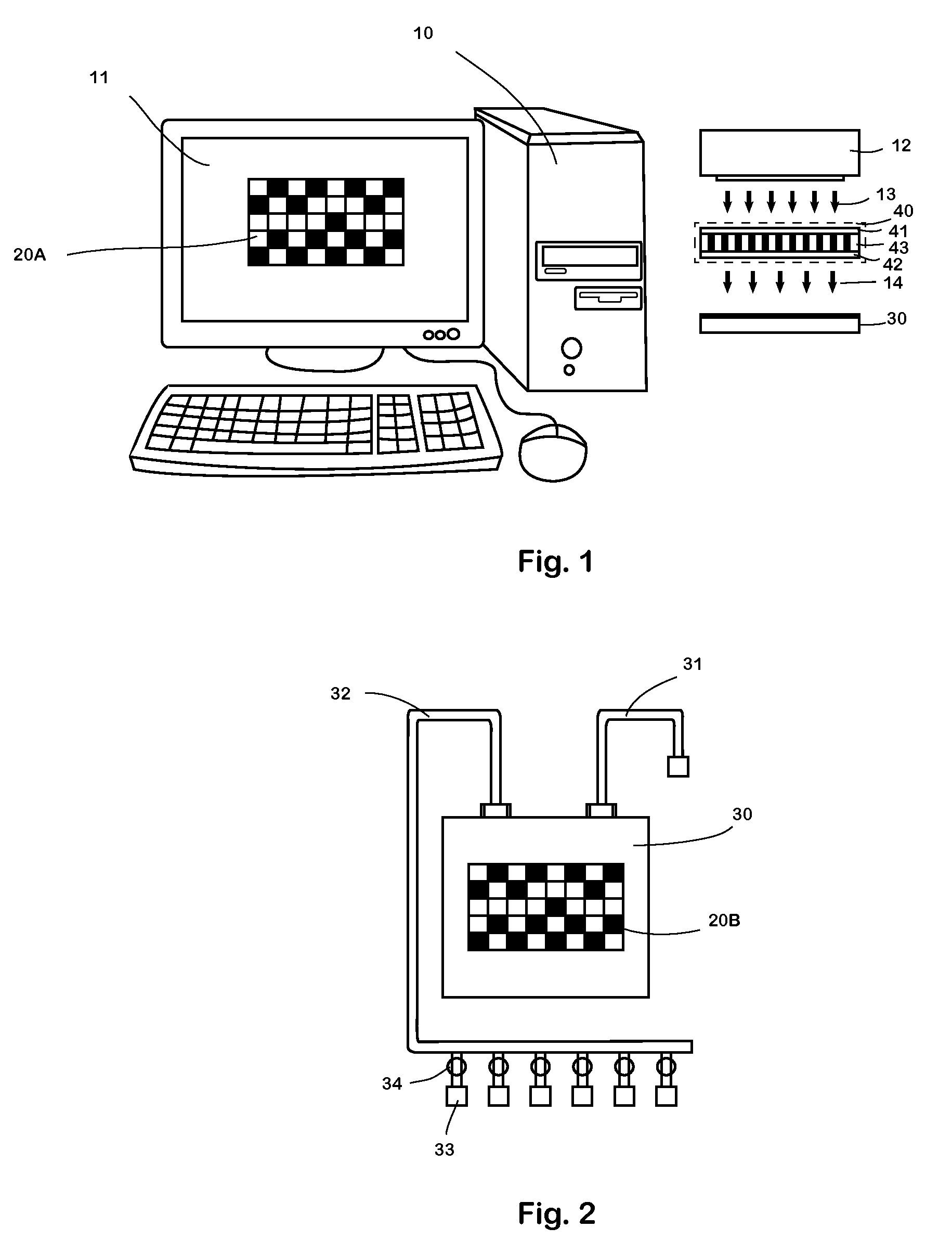
[0025]The present invention uses digital light processing technology with optical deprotection photochemistry to create a system and method for generating digital optical chemistry high diversity arrays. With this invention, the limitations of the traditional mask-based photolithographic processes are overcome by eliminating the need for one or more masks. The present invention is also based on the recognition that digital light processing technology can be used to pattern photoresist for the fabrication of substrates, e.g., semiconductor substrates. The present invention thus overcomes the problem of manufac...


PUM

PropertyMeasurementUnit
transparentaaaaaaaaaa
shrinkaaaaaaaaaa
semiconductoraaaaaaaaaa

Abstract

The invention teaches a system and method for catalyzing on a substrate. The system includes a light source and a digital light patterning device which is controlled by a controller coupled to a computer. The digital patterning device includes an array of liquid crystals, each of which being electronically controlled by the computer through the controller. When a liquid crystal is on, the light from the light source passes through the liquid crystal. When it is off, the light is blocked. According to the visual image pattern presented in the computer's interface, the array, wherein some crystals are on and some are off, shows a light pattern which is consistent with the visual image pattern on the computer screen. Accordingly, the patterned light is shed onto a substrate where the light catalyzes a chemical reaction proximate a substrate.

Description

FILED OF THE INVENTION[0001]The present invention generally relates to substrate patterning technology used in integrated semiconductor manufacturing. More particularly, the invention relates to a system and method for substrate patterning using a digital liquid crystal array coupled to a computer.BACKGROUND OF THE INVENTION[0002]In semiconductor design, and more specifically in substrate patterning of computer chips, a number of photolithographic masks were commonly used. The process required photolithographic protection of sections of a substrate. The masks protected the semiconductor layers during etching. Each layer required a unique mask design. The cost to implement this type of design was increased since printing and patterning each mask separately required a lengthened amount of time and cost.[0003]In integrated circuit design, technology advanced and discoveries were made involving the new apparatus for catalyzing a reaction on a substrate comprising a light source. In part...

Claims


Application Information

Patent Timeline
Patent Type & Authority Patents(United States)
IPC IPC(8): G02F1/1335G03F7/20
CPCG03F7/201G02F1/133509G03F7/2057
Inventor LI, CHENGZHANGLI, JIANBO
Owner AVENTGENE INC
Why Eureka
Try Eureka