Low temperature silicon nitride films using remote plasma CVD technology

a silicon nitride film, low temperature technology, applied in chemical vapor deposition coating, coating, metallic material coating process, etc., can solve the problems of poor step coverage of conventional silane-based plasma enhanced chemical vapor deposition (pecvd) silicon nitride films, high temperature requirement, and few engineering capabilities for film compositions and properties for different applications

Active Publication Date: 2017-02-28
APPLIED MATERIALS INC
View PDF8 Cites 203 Cited by
  • Summary
  • Abstract
  • Description
  • Claims
  • Application Information

AI Technical Summary

Problems solved by technology

The drawbacks, however, include a high temperature requirement (typically greater than 400° C.) and few capabilities to engineer film compositions and properties for different applications.
Alternatively, conventional silane-based plasma enhanced chemical vapor deposition (PECVD) silicon nitride films have poorer step coverage due to directionality of radicals' fluxes.
Additionally, tuning conformal layers to have desired film properties has also been difficult, particularly as the feature size decreases and the use of non-planar structures increases.

Method used


Image

  • Low temperature silicon nitride films using remote plasma CVD technology
  • Low temperature silicon nitride films using remote plasma CVD technology

Examples


Embodiment Construction

[0015]Embodiments of the present invention generally provide methods for forming a silicon nitride layer on a substrate. In one embodiment, a method of forming a silicon nitride layer using remote plasma chemical vapor deposition (CVD) at a temperature that is less than 300 degrees Celsius is disclosed. The precursors for the remote plasma CVD process include tris(dimethylamino)silane (TRIS), dichlorosilane (DCS), trisilylamine (TSA), bis-t-butylaminosilane (BTBAS), hexachlorodisilane (HCDS) or hexamethylcyclotrisilazane (HMCTZ).

[0016]Conformality of a layer is typically quantified by a ratio (which may be represented as a percentage) of the average thickness of a layer deposited on the sidewalls of a feature to the average thickness of the same deposited layer on the field, or upper surface, of the substrate. Layers deposited by the methods described herein are observed to have a conformality of greater than about 90%, such as 95% or greater, to about 100%.

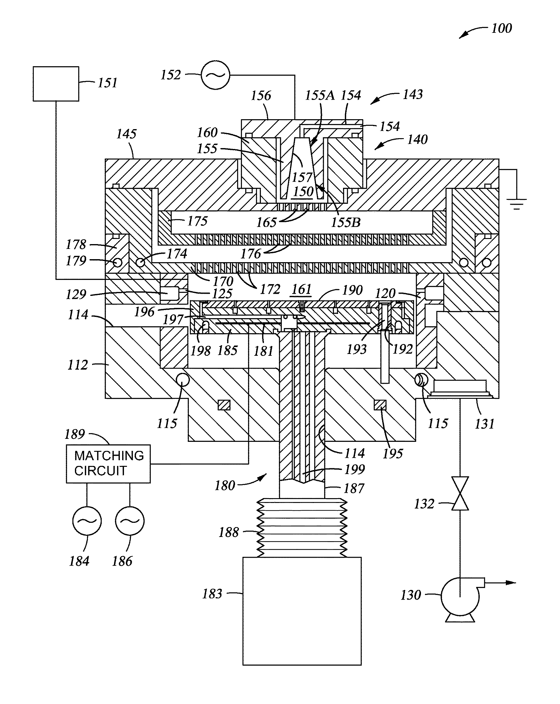
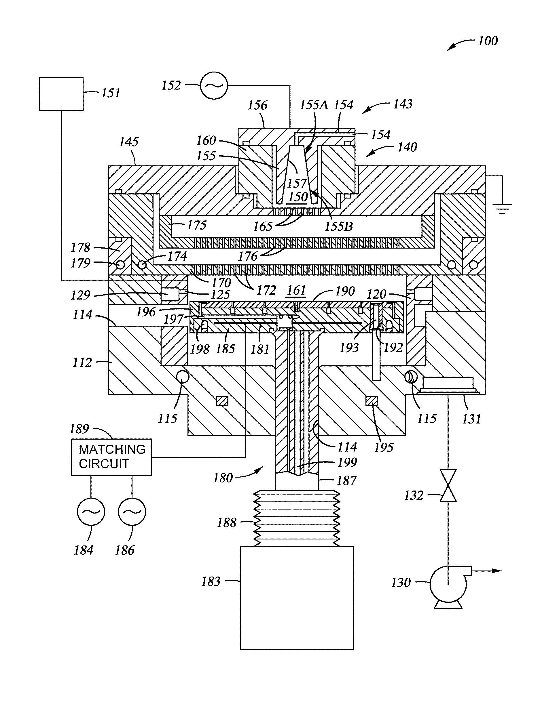
[0017]FIG. 1 is a cross-s...


PUM

PropertyMeasurementUnit
temperatureaaaaaaaaaa
refractive indexaaaaaaaaaa

Abstract

Embodiments of the present invention generally provide methods for forming a silicon nitride layer on a substrate. In one embodiment, a method of forming a silicon nitride layer using remote plasma chemical vapor deposition (CVD) at a temperature that is less than 300 degrees Celsius is disclosed. The precursors for the remote plasma CVD process include tris(dimethylamino)silane (TRIS), dichlorosilane (DCS), trisilylamine (TSA), bis-t-butylaminosilane (BTBAS), hexachlorodisilane (HCDS) or hexamethylcyclotrisilazane (HMCTZ).

Description

CROSS-REFERENCE TO RELATED APPLICATIONS[0001]This application claims priority to U.S. Provisional Patent Application Ser. No. 61 / 898,911, filed on Nov. 1, 2013, which herein is incorporated by reference.BACKGROUND[0002]Field[0003]Embodiments of the present invention generally relate to methods and processes for forming conformal silicon nitride films, including doped silicon nitride films, at low temperatures.[0004]Description of the Related Art[0005]The electronic device industry and the semiconductor industry continue to strive for larger production yields while increasing the uniformity of layers deposited on substrates having increasingly larger surface areas. These same factors in combination with new materials also provide higher integration of circuits per unit area on the substrate. As circuit integration increases, the need for greater uniformity and process control regarding layer characteristics rises.[0006]For example, ultra-large-scale integrated (ULSI) circuits typical...

Claims


Application Information

Patent Timeline
Patent Type & Authority Patents(United States)
IPC IPC(8): H01L21/02C23C16/452C23C16/44C23C16/34C23C16/455
CPCH01L21/0217C23C16/345C23C16/4411C23C16/452C23C16/45582H01L21/02211H01L21/02219H01L21/02222H01L21/02274
Inventor CHATTERJEE, AMITMALLICK, ABHIJIT BASUINGLE, NITIN K.
Owner APPLIED MATERIALS INC
Why Eureka
Try Eureka