Semiconductor device and method for fabricating the same

a technology of semiconductor devices and semiconductor components, applied in the direction of semiconductor devices, electrical equipment, transistors, etc., can solve the problems of reducing the reliability of semiconductor devices, and achieve the effects of high-speed response and high-speed operation, stable electric characteristics, and high reliability

Active Publication Date: 2017-03-21
SEMICON ENERGY LAB CO LTD
View PDF138 Cites 12 Cited by
  • Summary
  • Abstract
  • Description
  • Claims
  • Application Information

AI Technical Summary

Benefits of technology

[0012]For an increase in the area of an integrated circuit including a transistor, high-speed operation and high-speed response of the circuit are needed. An improvement in on-state characteristics (e.g., on-state current and field-effect mobility) of the transistor enables to provide a semiconductor device with higher performance, which is capable of high-speed operation and high-speed response.
[0013]In view of the above, an object of one embodiment of the present invention is to provide a semiconductor device capable of achieving high-speed response and high-speed operation by improving on-state characteristics of a transistor. Another object of one embodiment of the present invention is to fabricate a highly reliable semiconductor device showing stable electric characteristics.
[0015]It is preferable that the first oxide layer and the second oxide layer do not contain an impurity element such as silicon, which forms a level caused by impurity in the oxide semiconductor layer, as their main constituent elements. In the case where main elements of the first oxide layer and the second oxide layer are the same as a main element of the oxide semiconductor layer, scattering at an interface between the oxide semiconductor layer and the first oxide layer and at an interface between the oxide semiconductor layer and the second oxide layer is reduced, so that field-effect mobility can be increased. Oxides which contain the same element as their main constituent elements are used for the oxide semiconductor layer, the first oxide layer, and the second oxide layer, in which case trap levels at the interfaces can be reduced and variations in threshold voltage of a transistor due to change with time or a stress test can be reduced.
[0016]By the above method, a transistor can be formed without a contact between the oxide semiconductor layer and a layer containing an impurity element such as silicon. Thus, entry of the impurity element such as silicon to the oxide semiconductor layer can be prevented, thereby providing a highly reliable semiconductor device.
[0028]One embodiment of the present invention enables to provide a semiconductor device capable of high-speed response and high-speed operation. Another embodiment of the present invention enables to provide a highly reliable semiconductor device showing stable electric characteristics.

Problems solved by technology

Thus, electrical characteristics of the transistor are changed, which causes a reduction in reliability of a semiconductor device.

Method used


Image

  • Semiconductor device and method for fabricating the same
  • Semiconductor device and method for fabricating the same
  • Semiconductor device and method for fabricating the same

Examples


embodiment 1

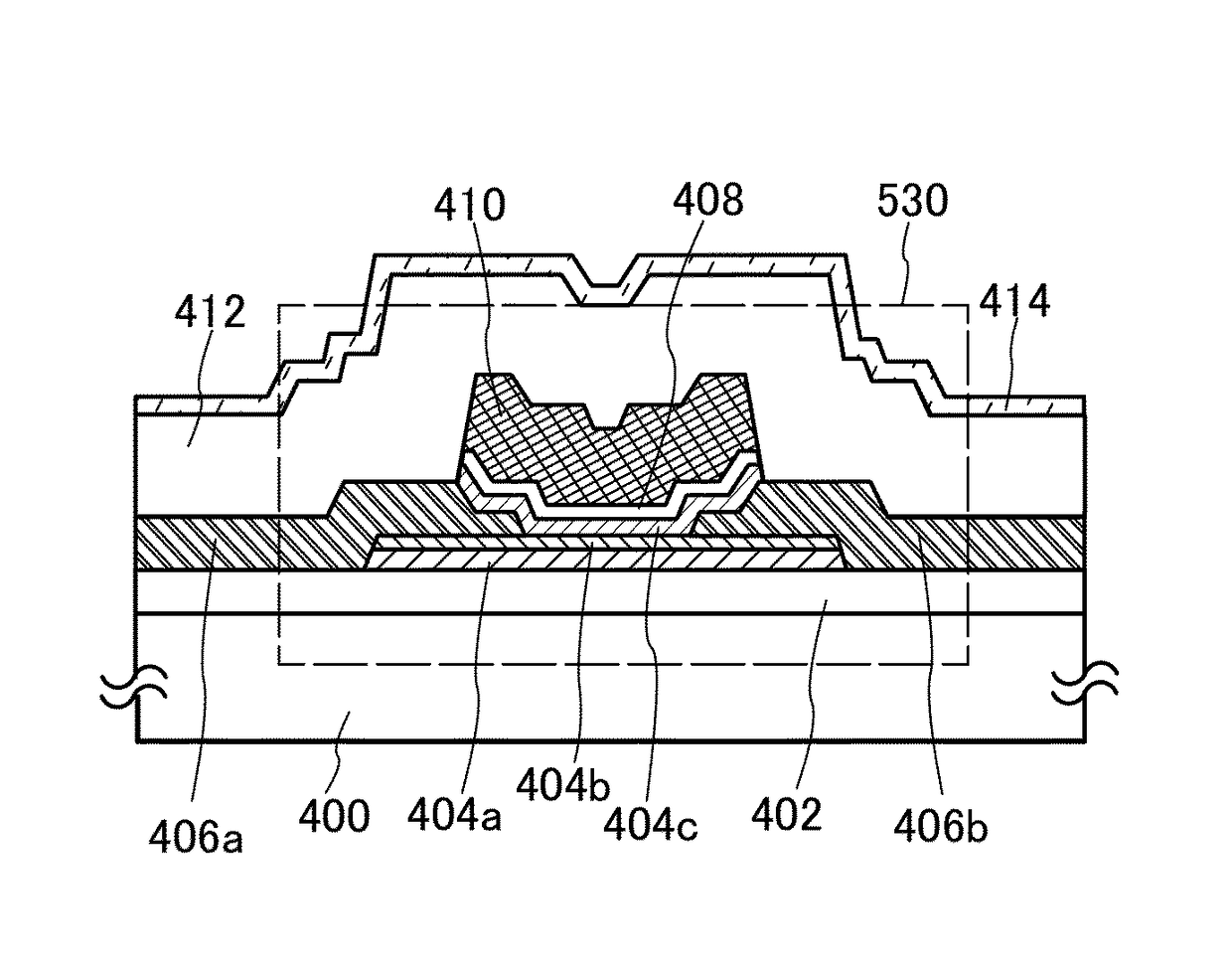
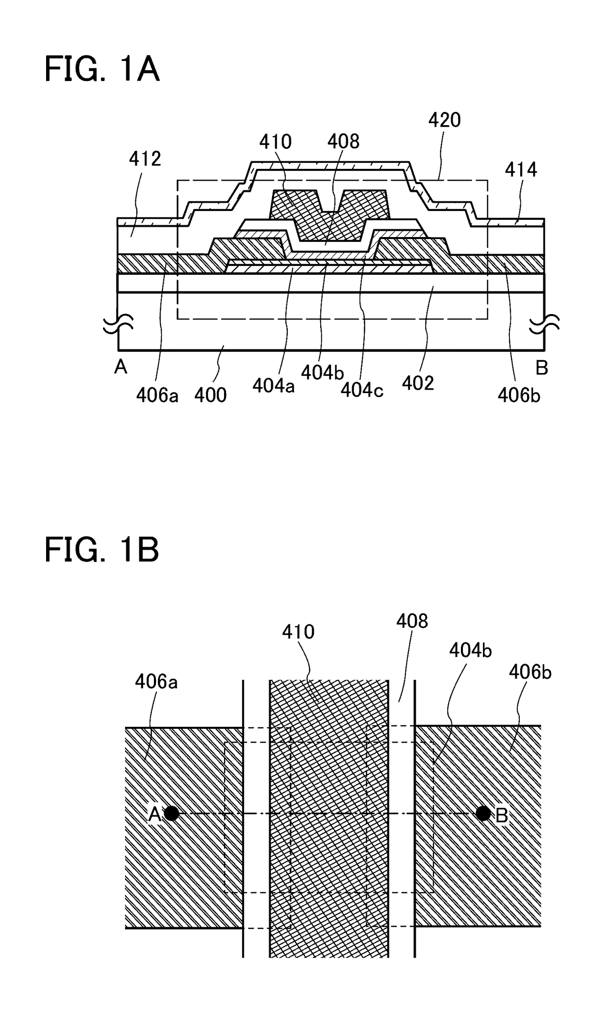
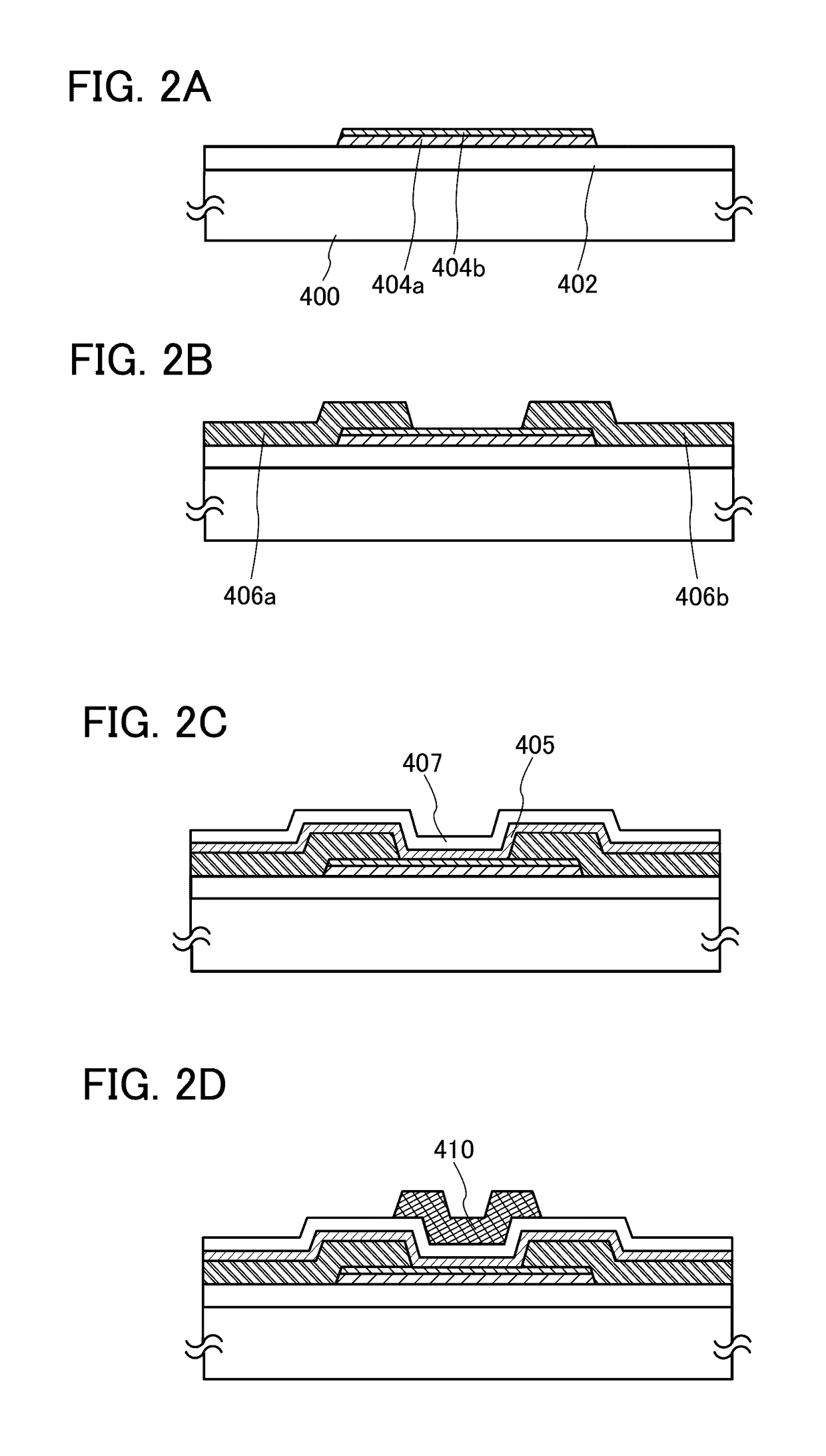
[0063]In this embodiment, a semiconductor device of one embodiment of the present invention will be described in detail with reference to drawings. FIGS. 1A and 1B illustrate a semiconductor device of one embodiment of the present invention. FIG. 1B is a top view illustrating the semiconductor device of one embodiment of the present invention, and FIG. 1A is a cross-sectional view taken along the dashed dotted line A-B in FIG. 1B.

[0064]A transistor 420 included in the semiconductor device includes a base insulating layer 402 over a substrate 400; a stack of a first oxide layer 404a and an oxide semiconductor layer 404b over the base insulating layer 402; a source electrode layer 406a and a drain electrode layer 406b over the first oxide layer 404a and the oxide semiconductor layer 404b; a second oxide layer 404c over the source electrode layer 406a and the drain electrode layer 406b; a gate insulating layer 408 over the second oxide layer 404c; a gate electrode layer 410 over the ga...

embodiment 2

[0183]In this embodiment, semiconductor devices each having a different structure from the structures in Embodiment 1 will be described. Note that in this embodiment, portions that are similar to the portions in Embodiment 1 are denoted by the same reference numerals, and detailed description thereof is omitted. FIGS. 6A and 6B illustrate a semiconductor device of this embodiment. FIG. 6B is a top view of the semiconductor device of this embodiment. FIG. 6A is a cross-sectional view taken along the dashed line C-D in FIG. 6B.

[0184]A transistor 520 illustrated in FIG. 6A includes the base insulating layer 402 over the substrate 400; the first oxide layer 404a and the oxide semiconductor layer 404b over the base insulating layer 402; the source electrode layer 406a and the drain electrode layer 406b over the first oxide layer 404a and the oxide semiconductor layer 404b; the second oxide layer 404c over the source electrode layer 406a and the drain electrode layer 406b; the gate insula...

embodiment 3

[0210]FIG. 11A illustrates an example of a circuit diagram of a NOR circuit, which is a logic circuit, as an example of the semiconductor device. FIG. 11B is a circuit diagram of a NAND circuit.

[0211]In the NOR circuit illustrated in FIG. 11A, p-channel transistors 801 and 802 each have a structure in which a single crystal silicon substrate is used for the channel formation region, and n-channel transistors 803 and 804 each have a structure similar to structures of the transistors the transistors described in Embodiments 1 and 2 in that an oxide semiconductor film is used for the channel formation region.

[0212]In the NOR circuit illustrated in FIG. 11A, a conductive layer controlling electrical characteristics of the transistor may be provided to overlap with a gate electrode layer with an oxide semiconductor film provided therebetween in each of the transistors 803 and 804. By controlling the potential of the conductive layer to GND, for example, the threshold voltages of the tran...


PUM


Abstract

The on-state characteristics of a transistor are improved and thus, a semiconductor device capable of high-speed response and high-speed operation is provided. A highly reliable semiconductor device showing stable electric characteristics is made. The semiconductor device includes a transistor including a first oxide layer; an oxide semiconductor layer over the first oxide layer; a source electrode layer and a drain electrode layer in contact with the oxide semiconductor layer; a second oxide layer over the oxide semiconductor layer; a gate insulating layer over the second oxide layer; and a gate electrode layer over the gate insulating layer. An end portion of the second oxide layer and an end portion of the gate insulating layer overlap with the source electrode layer and the drain electrode layer.

Description

BACKGROUND OF THE INVENTION[0001]1. Field of the Invention[0002]The present invention relates to a semiconductor device and a method for fabricating the semiconductor device.[0003]Note that a semiconductor device in this specification refers to all devices which can function by utilizing semiconductor characteristics, and electro-optical devices, semiconductor circuits, and electronic devices are all semiconductor devices.[0004]2. Description of the Related Art[0005]Attention has been focused on a technique for forming a transistor including a semiconductor thin film formed over a substrate having an insulating surface (also referred to as a thin film transistor). The transistor is applied to a wide range of electronic devices such as an integrated circuit (IC) or an image display device (a display device). A silicon-based semiconductor material is widely known as a material for a semiconductor thin film applicable to a transistor. As another material, a semiconductor material using...

Claims


Application Information

Patent Timeline
Patent Type & Authority Patents(United States)
IPC IPC(8): H01L29/786H01L29/66
CPCH01L29/7869H01L29/66969H01L29/78696H01L29/66742H01L27/14616H01L27/14689H01L27/1225H01L27/1255H01L21/02565H01L27/127
Inventor YAMAZAKI, SHUNPEISUZAWA, HIDEOMISASAGAWA, SHINYAKURATA, MOTOMUTSUBUKU, MASASHI
Owner SEMICON ENERGY LAB CO LTD
Why Eureka
Try Eureka