Check patentability & draft patents in minutes with Patsnap Eureka AI!

Crystal oscillation circuit and electronic timepiece

a crystal oscillation circuit and crystal oscillation circuit technology, applied in the field can solve the problems of crystal oscillation circuits that cannot oscillate, etc., and achieve the effect of stably short oscillation start time and low current consumption

Active Publication Date: 2017-04-25
ABLIC INC
View PDF4 Cites 0 Cited by
  • Summary
  • Abstract
  • Description
  • Claims
  • Application Information

AI Technical Summary

Benefits of technology

This configuration reduces current consumption and stabilizes oscillation start time, ensuring the circuit operates efficiently with minimal current consumption even with process variations.

Problems solved by technology

The related art crystal oscillation circuit is however accompanied by the following problems.
There is a possibility that when the current I9 is made small, the crystal oscillation circuit will not be capable of oscillating.
Further, there is a possibility that since the cutoff frequency of a high pass filter parasitically configured by the capacitor C2 and the constant current source 49 increases when the current I9 is made large, the crystal oscillation circuit will not be capable of oscillating.
Further, the crystal oscillation circuit was accompanied by a drawback that when the current I9 varied, the oscillation start time became long.

Method used


Image

  • Crystal oscillation circuit and electronic timepiece
  • Crystal oscillation circuit and electronic timepiece
  • Crystal oscillation circuit and electronic timepiece

Examples


Embodiment Construction

[0019]The present embodiment will hereinafter be described with reference to the accompanying drawings.

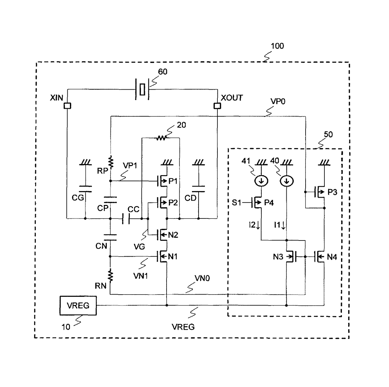
[0020]FIG. 1 is a circuit diagram illustrating a crystal oscillation circuit of the present embodiment.

[0021]The crystal oscillation circuit 100 is comprised of PMOS transistors P1 and P2, NMOS transistors N1 and N2, capacitors CP, CN, CC, CG and CD, a feedback resistor 20, resistors RP and RN, a bias circuit 50, a constant voltage circuit 10, and a crystal vibrator 60. The bias circuit 50 is comprised of constant current sources 40 and 41, PMOS transistors P3 and P4, and NMOS transistors N3 and N4.

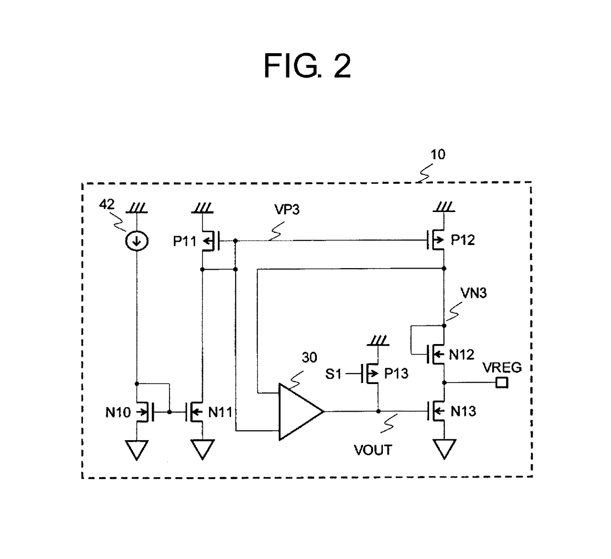
[0022]FIG. 2 is a circuit diagram illustrating one example of the constant voltage circuit of the crystal oscillation circuit of the present embodiment.

[0023]The constant voltage circuit 10 is comprised of a constant current source 42, PMOS transistors P11, P12, and P13, NMOS transistors N10, N11, N12, and N13, and a differential amplifier circuit 30.

[0024]A description will be made abou...


PUM


Abstract

To provide a crystal oscillation circuit low in current consumption and stably short in oscillation start time. A crystal oscillation circuit is equipped with a crystal vibrator, a feedback resistor, a bias circuit, a constant voltage circuit, and an oscillation inverter configured by a constant current inverter. The oscillation inverter is configured so as to be controlled by currents based on input signals from the bias circuit and the crystal vibrator and driven by an output voltage of the constant voltage circuit.

Description

RELATED APPLICATIONS[0001]This application claims priority under 35 U.S.C. §119 to Japanese Patent Application No. 2014-179420 filed on Sep. 3, 2014, the entire content of which is hereby incorporated by reference.BACKGROUND OF THE INVENTION[0002]Field of the Invention[0003]The present invention relates to a crystal oscillation circuit which is low in current consumption and stably short in oscillation start time.[0004]Background Art[0005]As a crystal oscillation circuit used in an electronic timepiece or the like, there has been known such a configuration as shown in Patent Document 1. FIG. 5 is illustrated in a range not departing from the crystal oscillation circuit shown in Patent Document 1.[0006]The crystal oscillation circuit 109 is comprised of PMOS transistors P31 and P32, NMOS transistors N31 and N32, capacitors C1, C2, C3 and C4, a feedback resistor 29, a constant current source 49, a constant voltage circuit 19, and a crystal vibrator 69.[0007]An oscillation inverter con...

Claims


Application Information

Patent Timeline
Patent Type & Authority Patents(United States)
IPC IPC(8): H03B11/00H03B5/30H03L5/00G04G3/00H03B5/36H03B5/32
CPCH03B5/364G04G3/00H03B5/30H03B5/32H03B5/366H03L5/00H03B2200/0062
Inventor WATANABE, KOTAROMITANI, MAKOTO
Owner ABLIC INC
Features
  • R&D
  • Intellectual Property
  • Life Sciences
  • Materials
  • Tech Scout
  • Unparalleled Data Quality
  • Higher Quality Content
  • 60% Fewer Hallucinations
Learn More