Charged particle beam device

a particle beam and charge technology, applied in the direction of electrical equipment, electrical discharge tubes, nuclear engineering, etc., can solve the problem of lowering the measurement accuracy of the apparatus, and achieve the effect of suppressing the position shift of the primary electron beam

Active Publication Date: 2017-06-13
HITACHI HIGH-TECH CORP
View PDF6 Cites 2 Cited by
  • Summary
  • Abstract
  • Description
  • Claims
  • Application Information

AI Technical Summary

Benefits of technology

[0014]According to the present invention, a processing apparatus and a processing method using a scanning electron microscope can be provided, which achieves deflection of secondary electrons / reflected electrons at a large angle and cancels out noises of an electromagnetic deflector and an electrostatic deflector to suppress a position shift of a primary electron beam caused by circuit noises in a primary beam / secondary beam separation circuit.

Problems solved by technology

Meanwhile, when a unit deflecting the secondary beam towards a predetermined direction affects the primary beam, a shift of a radiation position of the primary beam on the sample occurs, lowering a measurement accuracy of the apparatus.

Method used


Image

  • Charged particle beam device
  • Charged particle beam device
  • Charged particle beam device

Examples


first embodiment

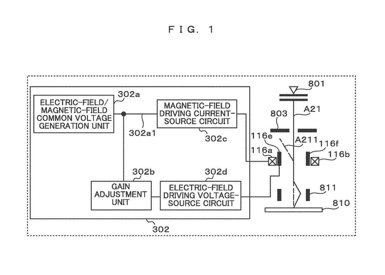
[0059]In the present embodiment, configurations as to the unit separating the primary beam and the second beam used in the orthogonal electromagnetic deflector are described, one of which enables a control signal generation unit of the voltage-source circuit controlling the electric-field deflector and a control signal generation unit of the current-source control circuit controlling the magnetic-field deflector to be formed as a common unit, and another of which adjusts a voltage signal controlling the electric field to satisfy the Wien condition with a current signal controlling the magnetic field as a reference.

[0060]A scanning electron beam metrology / inspection apparatus according to the present embodiment corresponds to an apparatus obtained by replacing the configuration of the control circuit of the orthogonal electromagnetic deflector for controlling the electric-field deflector and the magnetic-field deflector in the orthogonal electromagnetic deflector in the configuration...

second embodiment

[0071]A scanning electron beam metrology / inspection apparatus and a metrology / inspection method using the same according to the second embodiment of the present invention are described with reference to FIG. 2, in comparison with the conventional example.

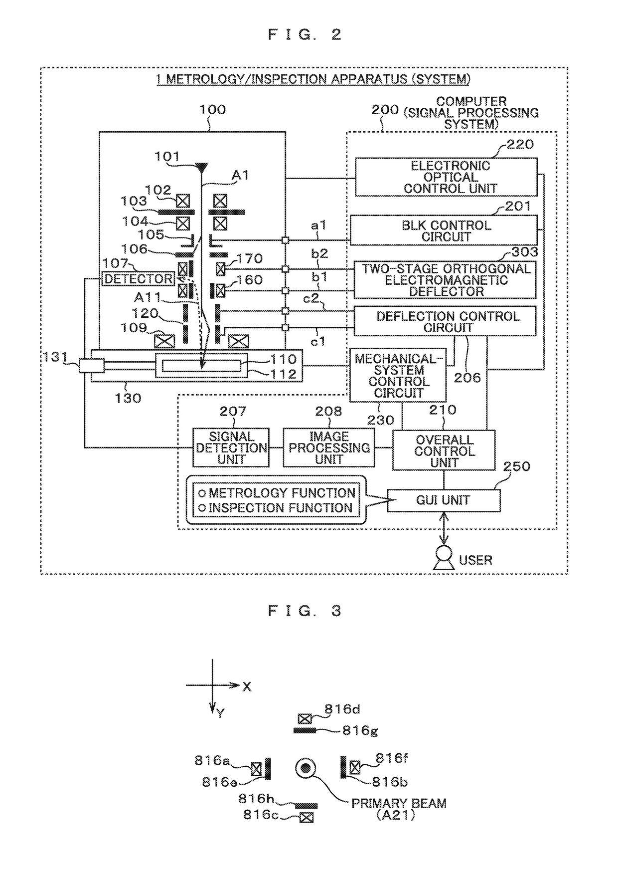
[0072]In the present embodiment, a unit in which orthogonal electromagnetic deflectors that separate primary electrons and secondary electrons and deflect a secondary beam are provided in two or more stages. FIG. 2 shows a case of a two-stage configuration.

[0073]This two-stage secondary beam deflecting unit has a feature of capable of solving a problem of chromatic aberration of a primary electron beam in a single-stage secondary beam deflecting unit.

[0074]The configuration in the second embodiment and an operation of correcting the chromatic aberration are described below.

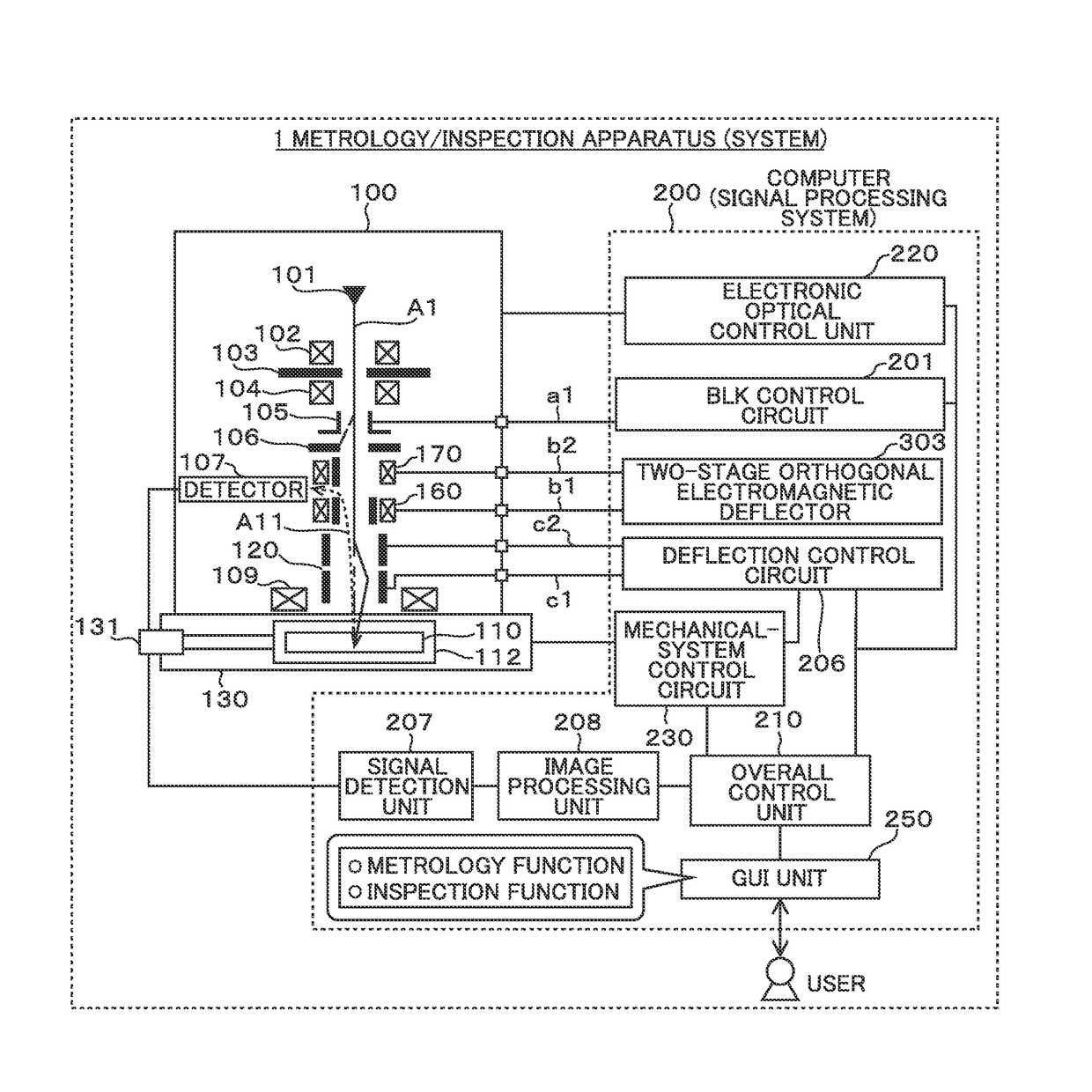
[Metrology / Inspection Apparatus (System)]

[0075]A configuration of a whole system including the metrology / inspection apparatus in this second embodiment is shown i...

third embodiment

[0096]Although the configuration described in the first embodiment only shows X-direction (or Y-direction) of the orthogonal electromagnetic deflector, a configuration of a scanning electron beam metrology / inspection apparatus in the present embodiment includes an orthogonal electromagnetic deflector and a control circuit thereof in both X-direction and Y-direction.

[0097]FIG. 10 is a block diagram showing the configuration of the control circuit of the orthogonal electromagnetic circuit according to the third embodiment of the present invention. As shown in FIG. 10, the control circuit of the orthogonal electromagnetic deflector described in the first embodiment is changed, in the present embodiment, to be formed by the voltage-source circuit and the current-source circuit that control the electric field and the magnetic field of the orthogonal electromagnetic deflector in each of X- and Y-directions. The signal generation units of the voltage-source circuit and the current-source c...


PUM


Abstract

A processing apparatus and a processing method are provided, which use a charged particle beam device that achieves defection of secondary electrons / reflected electrons at a large angle and cancels out noises of an electromagnetic deflector and an electrostatic deflector to suppress a position shift of a primary electron beam caused by circuit noises of a primary beam / secondary beam separation circuit. In the charged particle beam device that includes an electronic optical system radiating a concentrated electron beam onto a sample placed on a stage to perform scanning and captures an image of the sample, a reference signal and a signal generation unit of a voltage-source control signal applied to the electrostatic deflector generating the electrostatic deflector and a reference signal and a signal generation unit of a current-source control signal applied to the electromagnetic deflector generating a magnetic field are made common in an overlapping-electromagnetic-deflector control unit that controls a path of the secondary electrons / reflected electrons incident on a detector, and frequency characteristics and phase characteristics of the voltage control signal are coincident with those of the current-source control signal.

Description

TECHNICAL FIELD[0001]The present invention relates to a metrology / inspection apparatus that performs a process, e.g., measurement, observation, or inspection of a sample (an object), such as a semiconductor substrate (wafer), and a metrology / inspection method using the apparatus to perform the measurement or the inspection, for example. In particular, the present invention relates to a processing apparatus that captures an image of the sample using a scanning electron microscope apparatus (hereinafter, called SEM) as one of charged particle devices and performs the measurement, the observation, or the inspection and a metrology / inspection method thereof.BACKGROUND ART[0002]In a semiconductor manufacturing process, circuit patterns formed on a semiconductor substrate (wafer) are rapidly becoming finer, and importance of process monitoring that monitors whether or not the patterns are formed as designed, for example, is increasing. For example, measurement and inspection of the circui...

Claims


Application Information

Patent Timeline
Patent Type & Authority Patents(United States)
IPC IPC(8): H01J37/26G21K5/04H01J37/147H01J37/244H01J37/28
CPCH01J37/1472H01J37/244H01J37/28H01J2237/152H01J2237/1504H01J2237/2804H01J2237/2806H01J2237/1508H01J2237/1534
Inventor LI, WENKADOI, RYOIKEDA, KAZUKITAKAHASHI, HIROYUKIKAWANO, HAJIME
Owner HITACHI HIGH-TECH CORP
Why Eureka
Try Eureka