Strained stacked nanosheet FETS and/or quantum well stacked nanosheet

a nanosheet and nanosheet technology, applied in the direction of basic electric elements, electrical apparatus, semiconductor devices, etc., can solve the problems of limited roughness of channel/dielectric interface, high selective etches, and limited selectivity of etches for the si/sige system. the effect of low valu

Inactive Publication Date: 2017-07-18
SAMSUNG ELECTRONICS CO LTD
View PDF17 Cites 25 Cited by
  • Summary
  • Abstract
  • Description
  • Claims
  • Application Information

AI Technical Summary

Problems solved by technology

In addition, nanosheet architecture may compare favorably to the alternatives because the roughness of the channel / dielectric interface is limited by the precision of broad area epitaxial growth and selective etching instead of, e.g., lithography and anisotropic etching as is the case for FinFETs (field effect transistors)
One challenge is that highly selective etches must exist in order to ensure that the thickness of the nanosheet remains uniform from middle to end.
The selectivity of etches for the Si / SiGe system is limited to relatively low values due to the chemical similarity between Si and SiGe.
Another challenge facing adoption of nanosheets in advanced CMOS nodes is the introduction of strain into the channel (nanosheet channel layers) of the final structure.

Method used


Image

  • Strained stacked nanosheet FETS and/or quantum well stacked nanosheet
  • Strained stacked nanosheet FETS and/or quantum well stacked nanosheet
  • Strained stacked nanosheet FETS and/or quantum well stacked nanosheet

Examples


Embodiment Construction

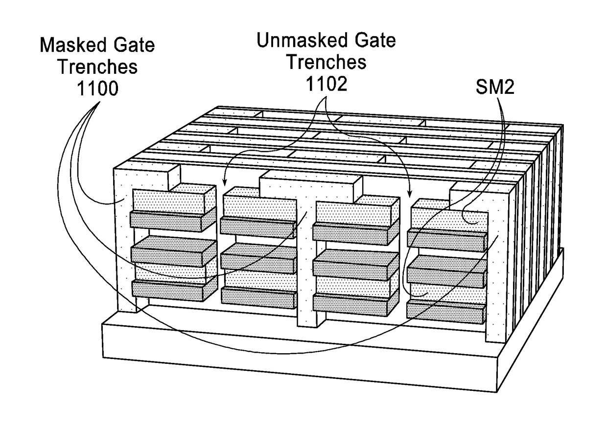
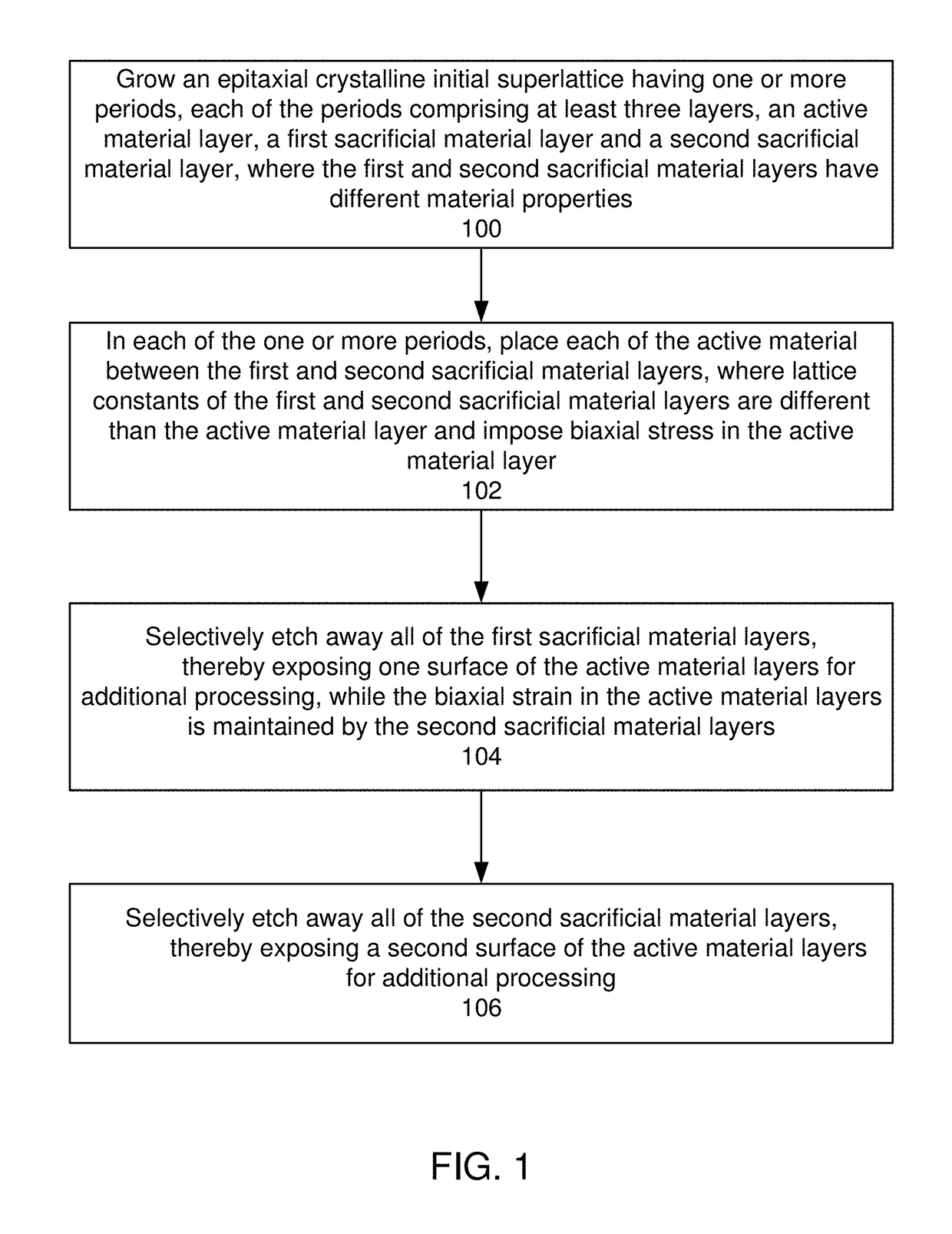
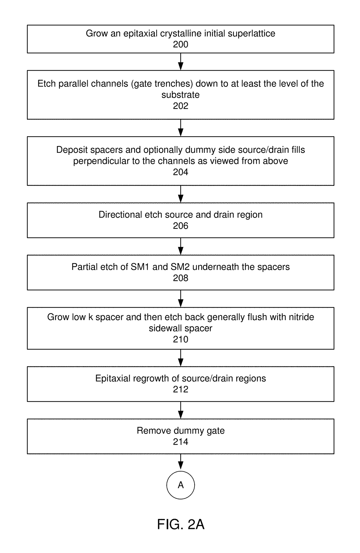
[0028]Reference will now be made in detail to the embodiments of the present general inventive concept, examples of which are illustrated in the accompanying drawings, wherein like reference numerals refer to the like elements throughout. The embodiments are described below in order to explain the present general inventive concept while referring to the figures.

[0029]Advantages and features of the present invention and methods of accomplishing the same may be understood more readily by reference to the following detailed description of embodiments and the accompanying drawings. The present general inventive concept may, however, be embodied in many different forms and should not be construed as being limited to the embodiments set forth herein. Rather, these embodiments are provided so that this disclosure will be thorough and complete and will fully convey the concept of the general inventive concept to those skilled in the art, and the present general inventive concept will only b...


PUM

PropertyMeasurementUnit
thicknessaaaaaaaaaa
thicknessaaaaaaaaaa
thicknessaaaaaaaaaa

Abstract

Exemplary embodiments provide for fabricating a biaxially strained nanosheet. Aspects of the exemplary embodiments include: growing an epitaxial crystalline initial superlattice having one or more periods, each of the periods comprising at least three layers, an active material layer, a first sacrificial material layer and a second sacrificial material layer, the first and second sacrificial material layers having different material properties; in each of the one or more periods, placing each of the active material layers between the first and second sacrificial material layers, wherein lattice constants of the first and second sacrificial material layers are different than the active material layer and impose biaxial stress in the active material layer; selectively etching away all of the first sacrificial material layers thereby exposing one surface of the active material for additional processing, while the biaxial strain in the active material layers is maintained by the second sacrificial material layers; and selectively etching away all of the second sacrificial material layers thereby exposing a second surface of the active material layers for additional processing.

Description

CROSS-REFERENCE TO RELATED APPLICATIONS[0001]This application claims the benefit of priority of provisional Patent Application Ser. No. 62 / 066,364 filed on Oct. 21, 2014. This application is also related to patent application Ser. No. 14 / 830,622 filed on Aug. 19, 2015, both assigned to the assignee of the present application and herein incorporated by reference.BACKGROUND[0002]Advanced CMOS nodes require multi-gate architectures in order to achieve sufficient electrostatic control to modulate current in short channels. A multi-level nanosheet device is a promising architecture for advanced nodes as it may offer excellent mobility, electrostatic control and possible layout enhancements. In addition, nanosheet architecture may compare favorably to the alternatives because the roughness of the channel / dielectric interface is limited by the precision of broad area epitaxial growth and selective etching instead of, e.g., lithography and anisotropic etching as is the case for FinFETs (fie...

Claims


Application Information

Patent Timeline
Patent Type & Authority Patents(United States)
IPC IPC(8): H01L21/8238H01L29/78H01L29/06H01L29/66
CPCH01L21/823807H01L21/823828H01L29/0665H01L29/66484H01L29/7847H01L29/42392H01L29/775H01L29/0673H01L29/20H01L29/22H01L29/78696
Inventor HATCHER, RYAN M.BOWEN, ROBERT C.RODDER, MARK S.OBRADOVIC, BORNA J.HONG, JOON GOO
Owner SAMSUNG ELECTRONICS CO LTD
Why Eureka
Try Eureka