Supercharge Your Innovation With Domain-Expert AI Agents!

Static random-access memory (SRAM) cell array and forming method thereof

Active Publication Date: 2017-08-08
UNITED MICROELECTRONICS CORP
View PDF2 Cites 12 Cited by
  • Summary
  • Abstract
  • Description
  • Claims
  • Application Information

AI Technical Summary

Benefits of technology

The present invention provides a method for improving the processing reliability and performance of a static random-access memory (SRAM) cell array. This is achieved by patterning a substrate with fin structures that include active fins and dummy fins, and then removing some of the dummy fins to create gaps between the fin structures. This results in a more stable and reliable device. Additionally, the invention allows for adjustment of the gaps between the active fins of adjacent pull-up FinFETs to improve performance and stability.

Problems solved by technology

Dynamic RAM is a simple structure, therefore having slow access speed and costing low.
Static RAM is a complex structure, therefore having high access speed and costing high, thereby it is often used as a memory providing low capacity but high speed such as a 256 KB or 512 KB cache memory built-in a central processing unit (CPU) of a personal computer.

Method used


Image

  • Static random-access memory (SRAM) cell array and forming method thereof
  • Static random-access memory (SRAM) cell array and forming method thereof
  • Static random-access memory (SRAM) cell array and forming method thereof

Examples


Embodiment Construction

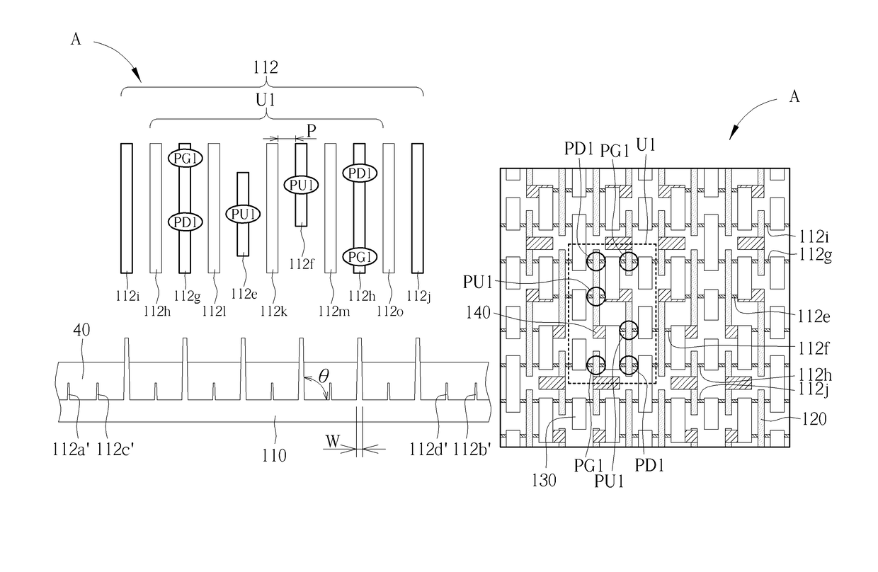
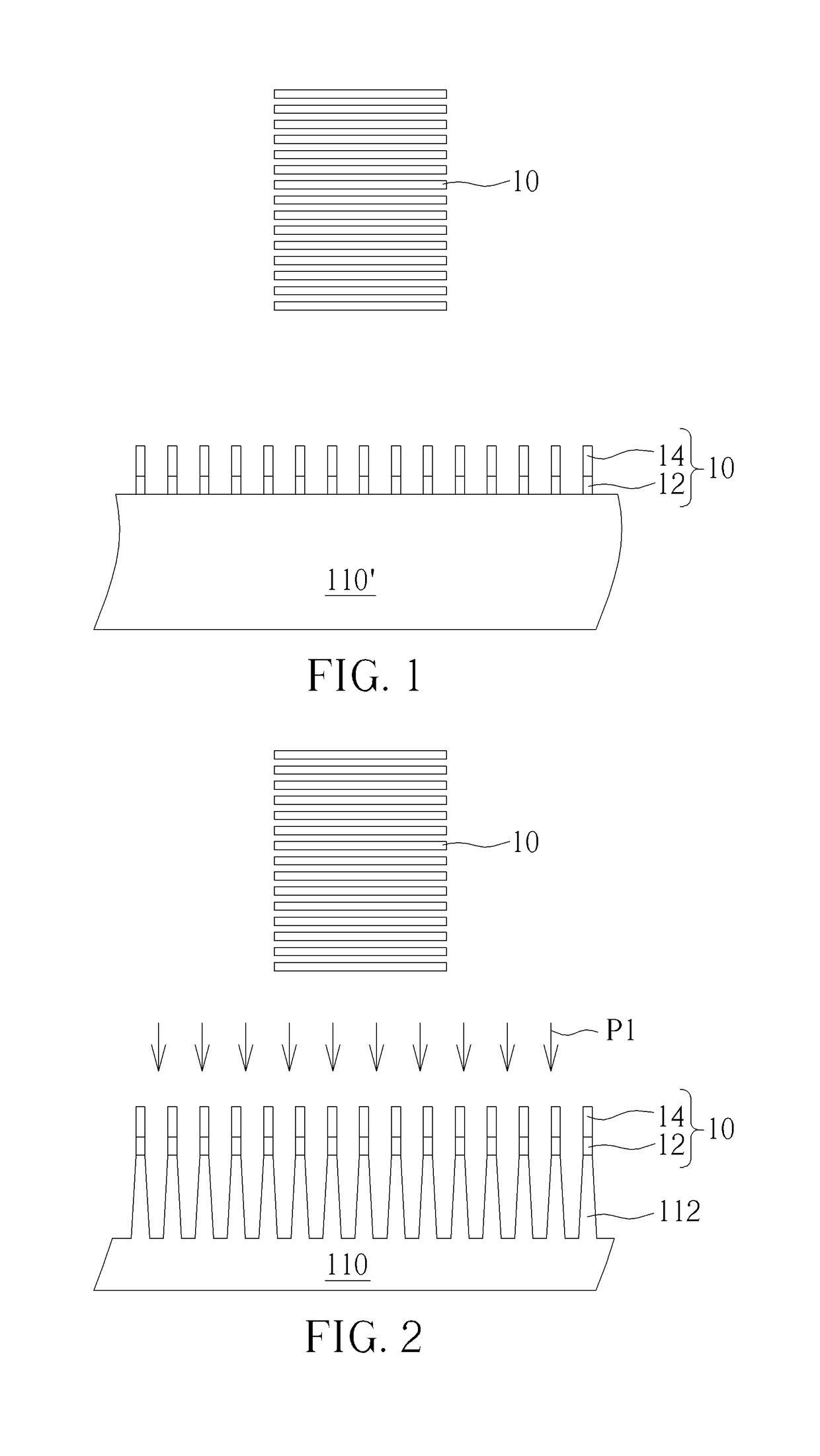
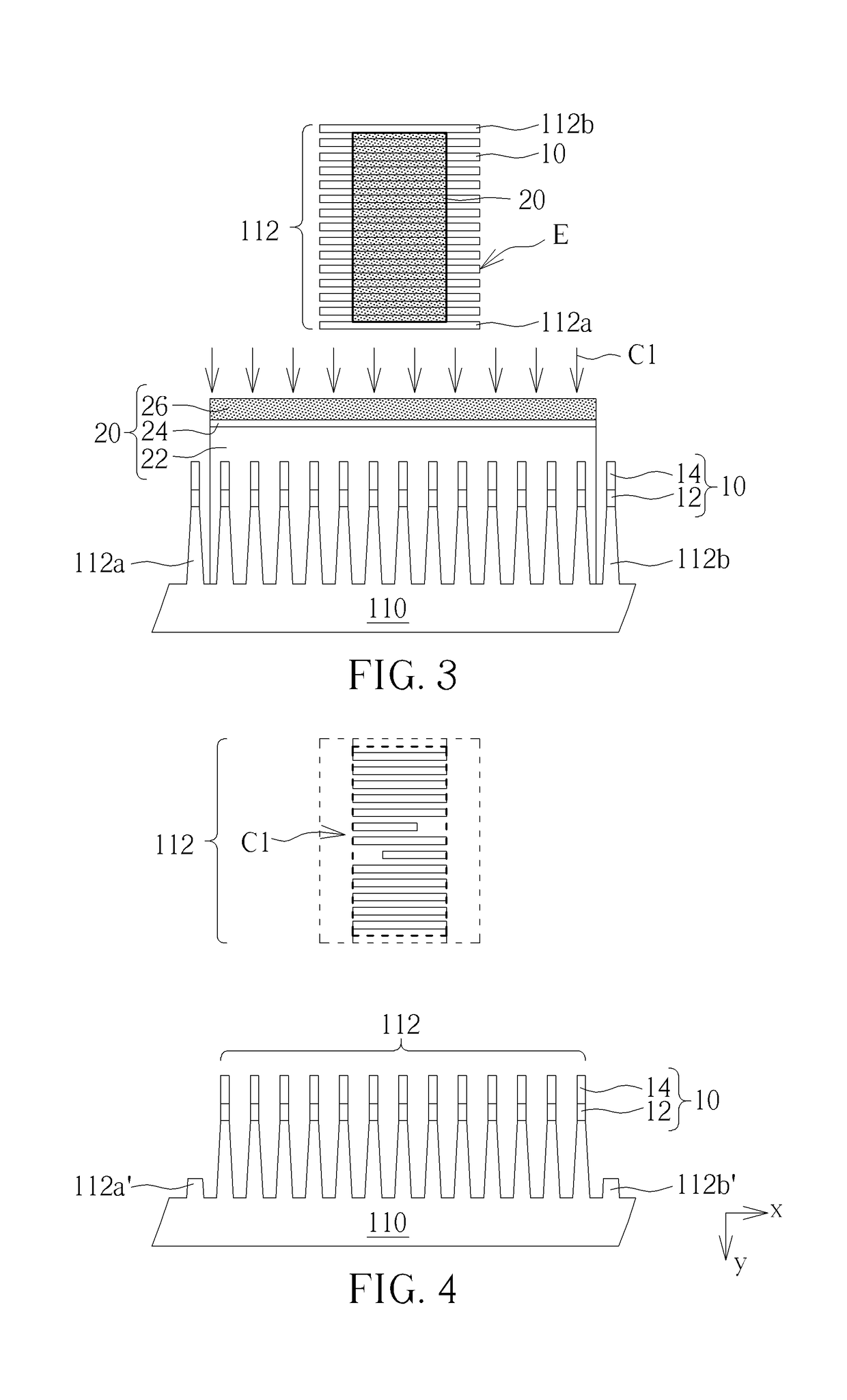
[0020]FIGS. 1-7 schematically depict top views and cross-sectional views of a method of forming a static random-access memory (SRAM) cell array according to an embodiment of the present invention. Please refer to FIGS. 1-2, in which a plurality of fin structures 112 are formed on a substrate 110. As shown in FIG. 1, a bulk bottom substrate 110′ is provided. A hard mask layer 10 is formed on the bulk bottom substrate 110′ and is patterned to define the location of the fin-shaped structures 112, which will be formed in the bulk bottom substrate 110′. In this case, the hard mask layer 10 is an oxide layer 12 and a nitride layer 14 stacked from bottom to top, but it is not limited thereto. As shown in FIG. 2, an etching process P1 is performed to form the fin-shaped structures 112 in the bulk bottom substrate 110′. Thus, the fin-shaped structures 112 located on the substrate 110 are formed completely. In one embodiment, the hard mask layer 10 is removed after the fin-shaped structures 1...


PUM


Abstract

A static random-access memory (SRAM) cell array forming method includes the following steps. A plurality of fin structures are formed on a substrate, wherein the fin structures include a plurality of active fins and a plurality of dummy fins, each PG (pass-gate) FinFET shares at least one of the active fins with a PD (pull-down) FinFET, and at least one dummy fin is disposed between the two active fins having two adjacent pull-up FinFETs thereover in a static random-access memory cell. At least a part of the dummy fins are removed. The present invention also provides a static random-access memory (SRAM) cell array formed by said method.

Description

BACKGROUND OF THE INVENTION[0001]1. Field of the Invention[0002]The present invention relates generally to a static random-access memory (SRAM) cell array and forming method thereof, and more specifically to a SRAM cell array applying dummy fins and forming method thereof.[0003]2. Description of the Prior Art[0004]Random access memory (RAM) can be operated to read data from it and write data into it. As the computers turn off, data disappears immediately. Since data in RAM can be altered easily, RAM is widely used as temporary data storage memory in personal computers. RAM can be classified into dynamic-type and static-type.[0005]A dynamic random access memory (DRAM: Dynamic RAM) stores one-bit data by one transistor paired with one capacitor, and electricity must be supported during operating to keep this data, thus called Dynamic RAM. Dynamic RAM is a simple structure, therefore having slow access speed and costing low. Thus, it is often used as a memory providing high capacity bu...

Claims


Application Information

Patent Timeline
IPC IPC(8): H01L21/336H01L27/11H01L29/78H01L29/66
CPCH01L27/1108H01L27/1116H01L29/785H01L29/6681H01L21/823431H01L27/0886H10B10/12H10B10/18
Inventor HUANG, CHUN-HSIENKUO, YU-TSEWANG, SHU-RU
Owner UNITED MICROELECTRONICS CORP
Features
  • R&D
  • Intellectual Property
  • Life Sciences
  • Materials
  • Tech Scout
  • Unparalleled Data Quality
  • Higher Quality Content
  • 60% Fewer Hallucinations
Learn More