
Method of growing nitride semiconductor layer

a technology of nitride and semiconductor layer, which is applied in the direction of semiconductor devices, basic electric elements, electrical apparatus, etc., can solve the problems of cracks, difficult to use the single crystal of gan to manufacture devices, and difficulty in mass production of single crystal of gan

Active Publication Date: 2017-08-22
SAMSUNG ELECTRONICS CO LTD
View PDF62 Cites 1 Cited by
  • Summary
  • Abstract
  • Description
  • Claims
  • Application Information

AI Technical Summary

Benefits of technology

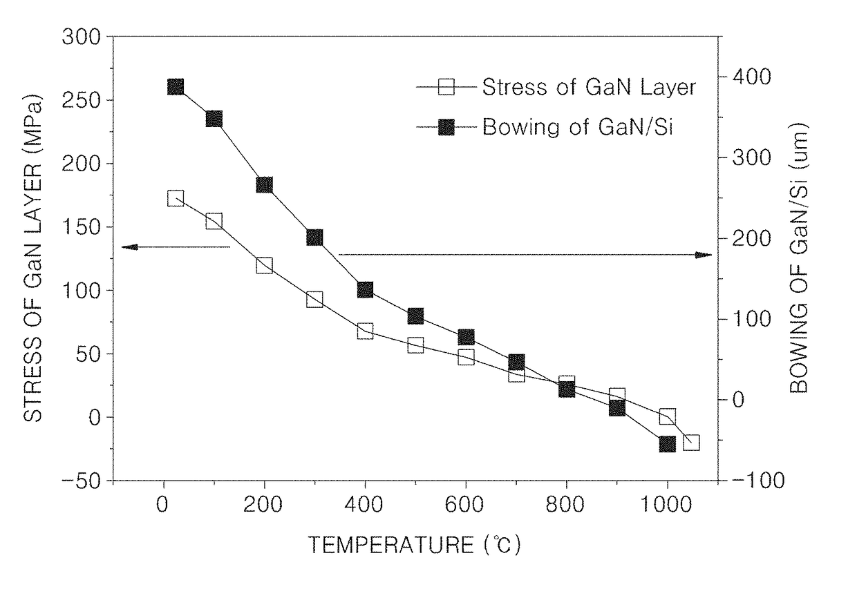
[0012]Example embodiments provide methods of growing a nitride semiconductor that may reduce crack generation and / or propagation or bowings due to the presence of a tensile stress caused by a difference in a lattice constant or a thermal expansion coefficient when the nitride semiconductor is grown on a substrate.

Problems solved by technology

Because growth of a single crystal of GaN in a liquid phase requires a relatively high temperature equal to or higher than about 1500° C. and a nitrogen atmosphere of about 20,000 atm due to a relatively high nitrogen vapor pressure at a melting point, mass producing the single crystal of GaN may be difficult.
Also, because a size of the single crystal of GaN that may be currently used is about 100 mm2, using the single crystal of GaN to manufacture a device may be difficult.
However, when GaN grown on a silicon substrate directly contacts silicon, the silicon may diffuse into the GaN, a surface of the silicon substrate may be etched to cause meltback, and cracks may occur due to a tensile stress when the GaN is grown on the silicon substrate due to a difference in a thermal expansion coefficient and a lattice constant between the silicon and the GaN.
To solve this problem, although a method of growing GaN on a silicon substrate by using a graded buffer layer is used, the method may include growing a GaN thin film but has a limitation in growing a thick GaN layer.

Method used


Image

  • Method of growing nitride semiconductor layer
  • Method of growing nitride semiconductor layer
  • Method of growing nitride semiconductor layer

Examples


Embodiment Construction

[0034]Example embodiments will hereinafter be described in further detail with reference to the accompanying drawings, in which various embodiments are shown. This disclosure may, however, be embodied in many different forms and should not be construed as limited to example embodiments set forth herein. In the drawings, the thicknesses of layers and regions are exaggerated for clarity. Like reference numerals in the drawings denote like elements, and thus their description will be omitted.

[0035]It will be understood that, although the terms “first”, “second”, etc. may be used herein to describe various elements, components, regions, layers and / or sections, these elements, components, regions, layers and / or sections are not to be limited by these terms. These terms are only used to distinguish one element, component, region, layer or section from another element, component, region, layer or section. Thus, a first element, component, region, layer or section discussed below could be t...


PUM

PropertyMeasurementUnit
temperatureaaaaaaaaaa

Abstract

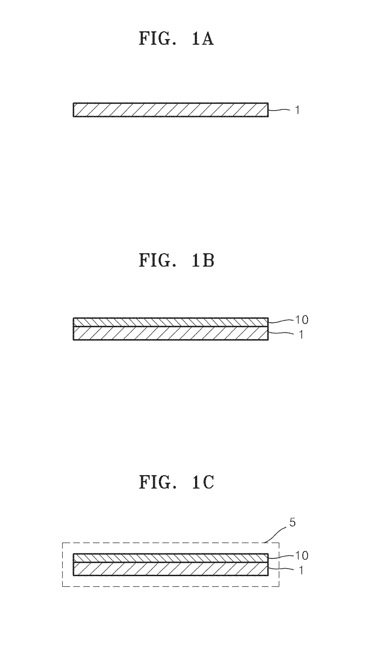
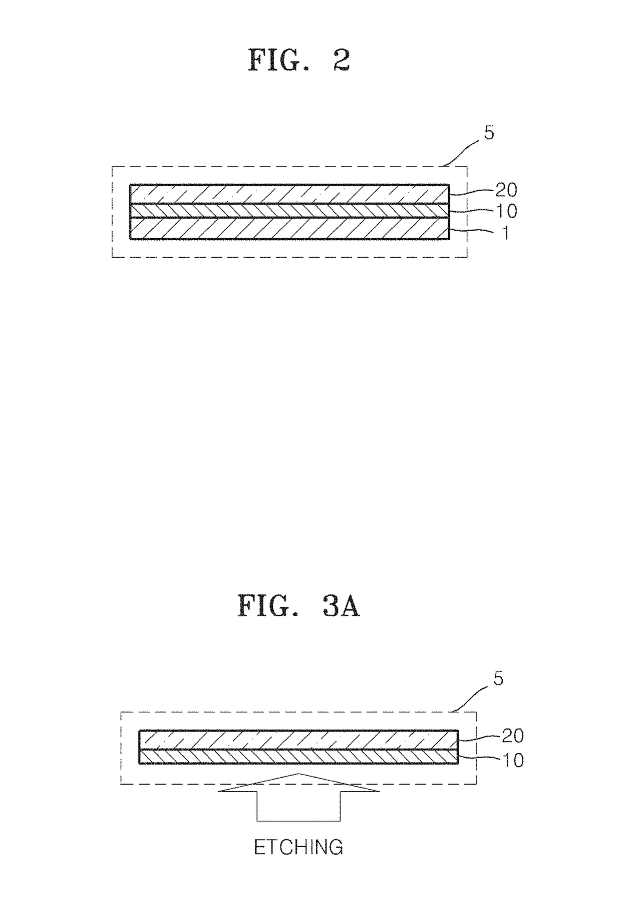
A method of growing a nitride semiconductor layer may include preparing a substrate in a reactor, growing a first nitride semiconductor on the substrate at a first temperature, the first nitride semiconductor having a thermal expansion coefficient different from a thermal expansion coefficient of the substrate, and removing the substrate at a second temperature.

Description

CROSS-REFERENCE TO RELATED APPLICATIONS[0001]This application claims the benefit of Korean Patent Application No. 10-2012-0003085, filed on Jan. 10, 2012, in the Korean Intellectual Property Office, the disclosure of which is incorporated herein in its entirety by reference.BACKGROUND[0002]1. Field[0003]Example embodiments relate to methods of growing a nitride semiconductor layer.[0004]2. Description of the Related Art[0005]Electronic industries using nitride semiconductors have drawn attention as fields suitable for development and growth of green industries. In particular, GaN, a nitride semiconductor, is widely used to manufacture a blue light-emitting diode from among red, green, and blue light-emitting diodes, which are essential elements of high power electronic component devices including a light-emitting diode (LED). A blue LED using GaN is more desirable in terms of brightness, lifespan, and internal quantum efficiency to conventional blue light-emitting devices using a se...

Claims


Application Information

Patent Timeline
Patent Type & Authority Patents(United States)
IPC IPC(8): H01L21/20H01L21/02H01L21/36H01L29/20H01L21/3065
CPCH01L21/02389H01L21/0254H01L21/02381H01L21/02439H01L21/02458H01L21/02505H01L21/02664H01L29/2003H01L21/3065H01L21/20
Inventor PARK, SUNG-SOOLEE, MOON-SANGPARK, YOUNG-SOO
Owner SAMSUNG ELECTRONICS CO LTD
Learn More