
Lossless snubber circuit and operation method thereof

a snubber circuit and lossless technology, applied in the field of lossless snubber circuit and an operation method thereof, can solve the problems of increasing the loss of the switch transistor, affecting the efficiency of the entire circuit, and the snubber circuit cannot efficiently depress the voltage spike, so as to reduce the power consumption of the devi

Active Publication Date: 2017-09-12
VERTIV CORP
View PDF7 Cites 0 Cited by
  • Summary
  • Abstract
  • Description
  • Claims
  • Application Information

AI Technical Summary

Benefits of technology

The invention aims to reduce voltage spikes and power consumption in a circuit. It does this by using a large capacitor to absorb voltage spikes caused by the turn-off of a switch transistor. When the switch transistor is turned on, the capacitor releases electric charges to another capacitor in the circuit, avoiding voltage stress and reducing power consumption.

Problems solved by technology

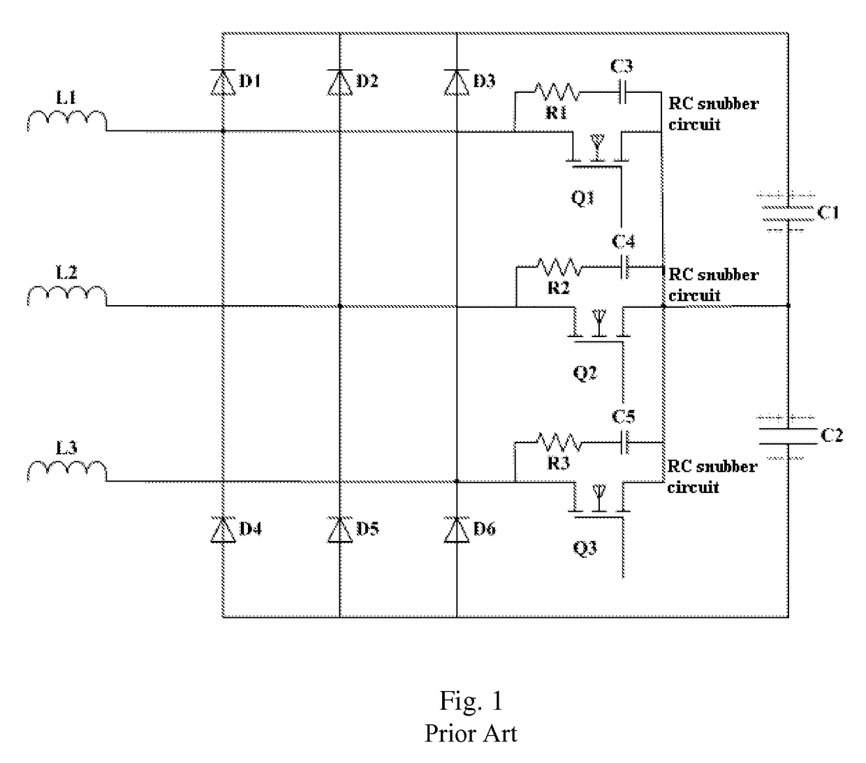
In the case where the capacitance of the capacitor C3 is small, while the voltage spike generated at the moment when the switch transistor Q1 is turned off is too large, the RC snubber circuit can not efficiently depress the voltage spike.
If the released electric charges cannot be consumed by the inductor R1, the residual electric charges may influence the output junction capacitance of the switch transistor Q1, increase the loss of the switch transistor, and affect the efficiency of the entire circuit.
Therefore, it can be seen that, in the existing RC snubber circuit, the problems of effective depression to the voltage spike generated when the switch transistor Q1 is turned off and the voltage stress difference when the switch transistor Q1 is turned on cannot be solved simultaneously.

Method used


Image

  • Lossless snubber circuit and operation method thereof
  • Lossless snubber circuit and operation method thereof
  • Lossless snubber circuit and operation method thereof

Examples


first embodiment

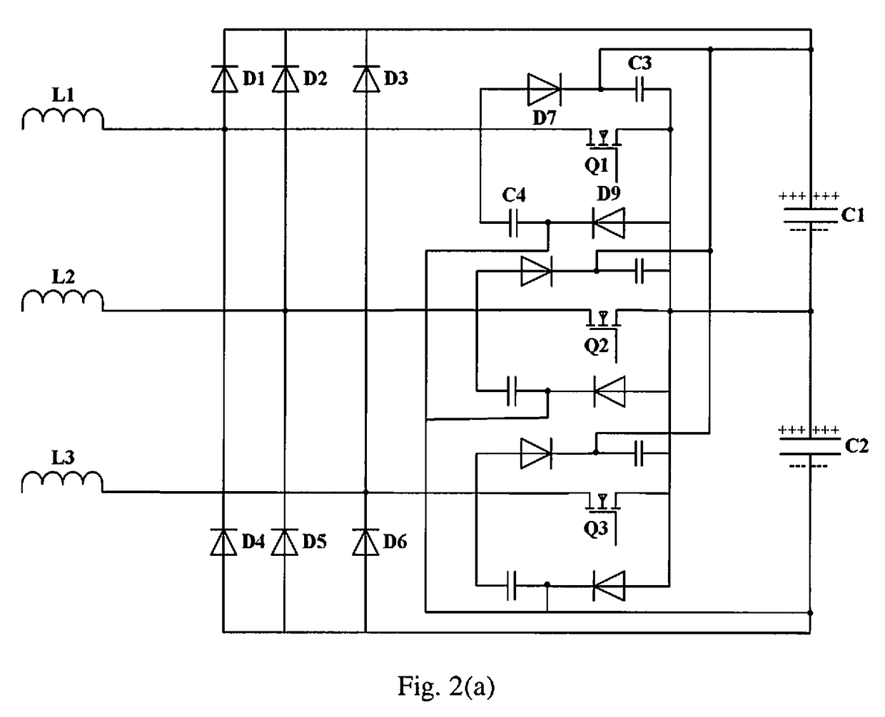
[0033]FIG. 2(a) is a structural schematic view of a lossless snubber circuit according to a first embodiment of the invention. As shown in FIG. 2(a), the lossless snubber circuit is applied to a circuit for each phase of a three-phase Vienna circuit structure and includes a first snubber circuit. The first snubber circuit includes a first diode D7 and a capacitor C3.

[0034]The anode of the first diode D7 in the first snubber circuit is connected to the drain of a switch transistor Q1, and one terminal of the capacitor C3 in the first snubber circuit is connected to the source of the switch transistor Q1.

[0035]The cathode of the first diode D7 in the first snubber circuit is connected to the other terminal of the capacitor C3 in the first snubber circuit, the connection point between the cathode of the first diode D7 in the first snubber circuit and the capacitor C3 in the first snubber circuit is connected to the positive electrode of a first capacitor C1 in the three-phase Vienna st...

second embodiment

[0049]The second embodiment of the invention provides an operation method for a lossless snubber circuit which includes the following.

[0050]First Case

[0051]The lossless snubber circuit includes a first snubber circuit. The first snubber circuit includes a first diode D7 and a capacitor C3 which are connected in a way as that of the first snubber circuit shown in FIG. 2(a).

[0052]The capacitance of the capacitor C3 is smaller than the capacitance of the first capacitor C1 in the three-phase Vienna structure.

[0053]The capacitance of the capacitor C3 in the first snubber circuit may be determined according to the voltage spike generated at the moment when the switch transistor Q1 is turned off, or may be determined as required, which is not limited thereto.

[0054]FIG. 3 is a schematic view of an operation method of the lossless snubber circuit. As shown in FIG. 3, in the case where an input voltage is a forward voltage and the anode of the first diode D7 in the first snubber circuit is c...

third embodiment

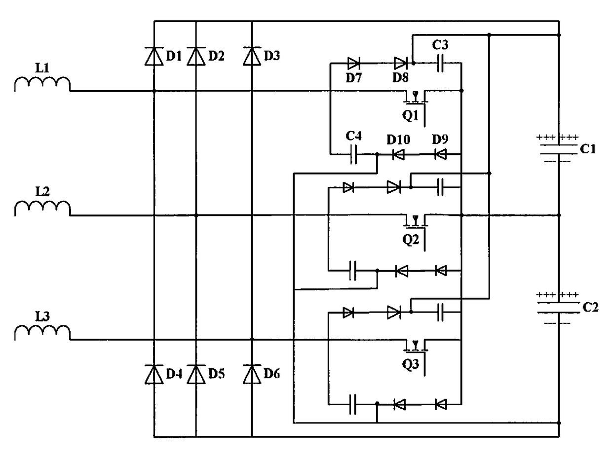
[0085]A lossless snubber circuit is included in a three-phase Vienna structure. The lossless snubber circuit includes a first snubber circuit and a second snubber circuit. The first snubber circuit includes a first diode D7 and a capacitor C3. The second snubber circuit includes a second diode D9 and a capacitor C4.

[0086]In the lossless snubber circuit, the anode of the first diode D7 in the first snubber circuit is connected to the drain of the switch transistor Q1. The cathode of the first diode D7 is connected to one terminal of the capacitor C3. The other terminal of the capacitor C3 in is connected to the source of the switch transistor Q1. The connection point between the cathode of the first diode D7 and one terminal of the capacitor C3 is connected to the positive electrode of the capacitor C1 in the three-phase Vienna structure.

[0087]In the lossless snubber circuit, the anode of the first diode D9 in the second snubber circuit is connected to the source of the switch transi...


PUM


Abstract

The present invention discloses a lossless snubber circuit and an operation method thereof. The lossless snubber circuit includes a first snubber circuit. The first snubber circuit includes a first diode (D7) and a capacitor (C3). The capacitance of the capacitor (C3) is big enough so that a voltage spike generated at the moment when a switch transistor (Q1) is turned off is depressed by charging the capacitor (C3). When the switch transistor (Q1) is on, the electric charges released by the capacitor (C3) are directed to a first capacitor (C1) in a three-phase Vienna structure, so as to avoid the problem of voltage stress difference caused by the large quantity of electric charges released by the capacitor (C3) flowing back to the switch transistor (Q1).

Description

FIELD OF THE INVENTION[0001]The present invention generally relates to the field of wireless communication, and particularly to a lossless snubber circuit and an operation method thereof.BACKGROUND OF THE INVENTION[0002]In electrical field, there is an ideal topology circuit structure, i.e. the three-phase Vienna structure. Circuits of such structure have advantages such as small input current ripple, less device requirements, simple control and low cost, and thus are widely applied in the case of three-phase alternating current high power input.[0003]A circuit diagram of the three-phase Vienna circuit structure is shown in FIG. 1. The circuit has circuits for three phases. The connection structure of the circuit for one phase is: a inductor L1 is connected to the anode of a diode D1 and connected to the cathode of a diode D4; the cathode of the diode D1 is connected to the positive electrode of a capacitor C1; the anode of the diode D4 is connected to the negative electrode of a ca...

Claims


Application Information

Patent Timeline
Patent Type & Authority Patents(United States)
IPC IPC(8): H02H3/20H02M1/34H02M7/155
CPCH02M1/34H02M7/155H02M2001/348H02M1/348
Inventor WANG, MENG
Owner VERTIV CORP
Learn More