Method of forming patterned mask layer

Active Publication Date: 2017-10-03
UNITED MICROELECTRONICS CORP
View PDF5 Cites 3 Cited by
  • Summary
  • Abstract
  • Description
  • Claims
  • Application Information

AI Technical Summary

Benefits of technology

[0007]According to the method of forming the patterned mask layer in the present invention, a part of each of the spacers is removed by the trimming process with the patterned protection layer formed on the top surfaces of the space

Problems solved by technology

The development of semiconductor integrated circuit technology progresses continuously and circuit designs in products of the new generation become smaller and more complicated than those of the former generation.
The size and

Method used


Image

  • Method of forming patterned mask layer
  • Method of forming patterned mask layer
  • Method of forming patterned mask layer

Examples


Embodiment Construction

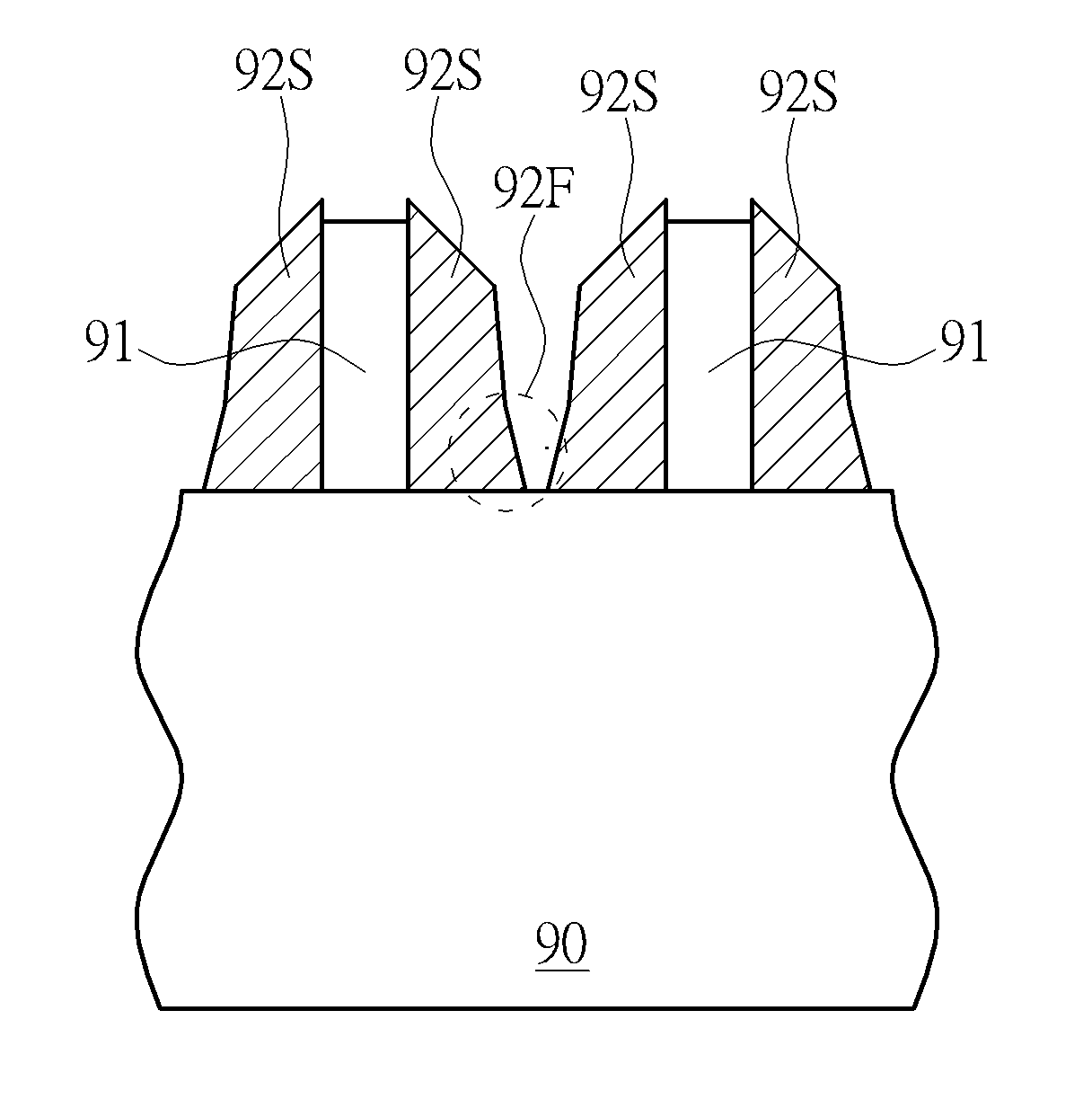
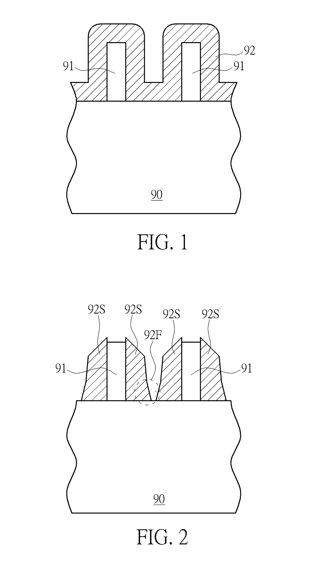
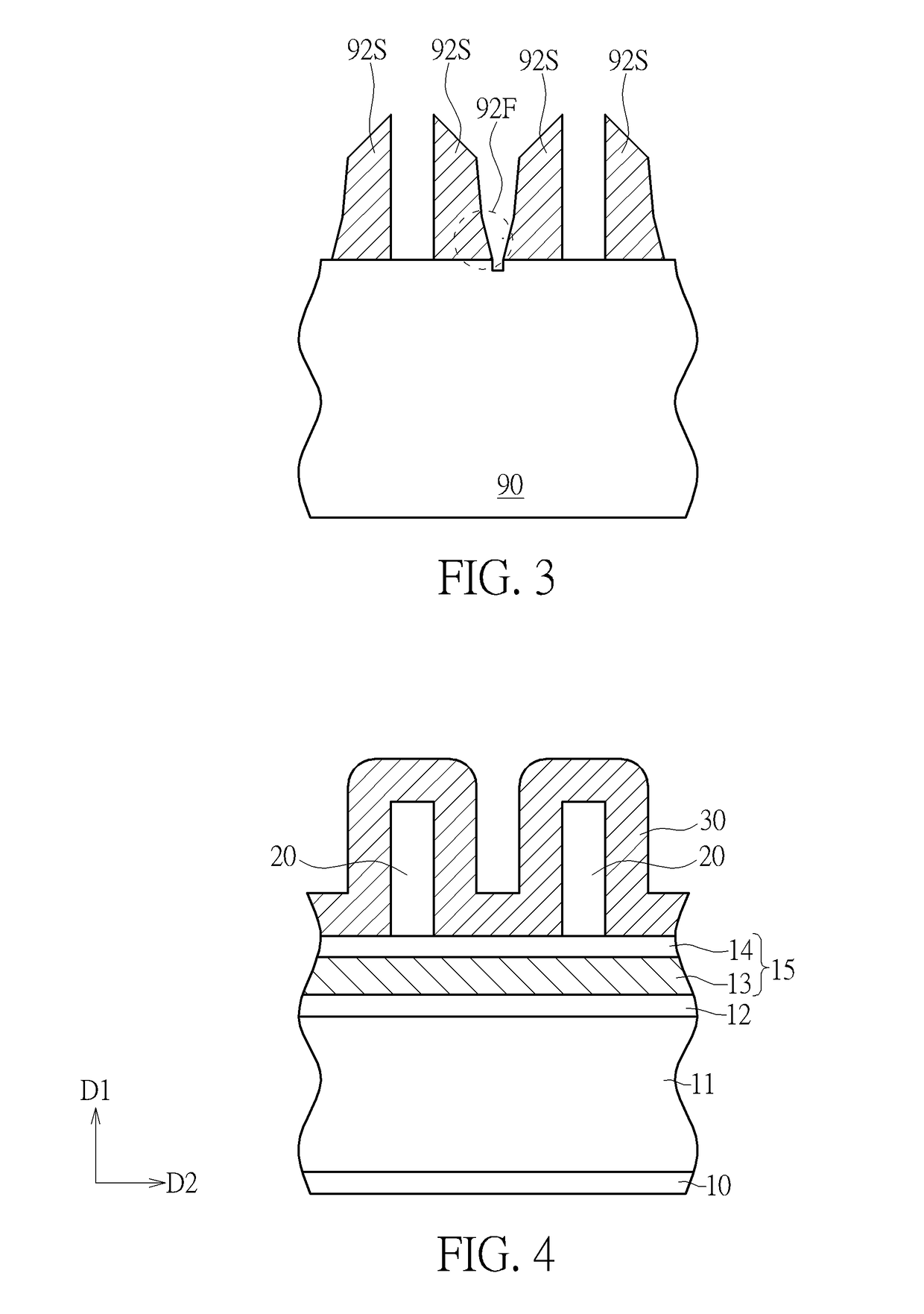
[0021]Please refer to FIGS. 4-12. FIGS. 4-12 are schematic drawings illustrating a method of forming a patterned mask layer according to an embodiment of the present invention. The method of forming the patterned mask layer in this embodiment includes the following steps. As shown in FIG. 4, a mask layer 15 is provided. The mask layer 15 may be formed on a semiconductor substrate (not shown), and the semiconductor substrate may include silicon substrate, epitaxial substrate, silicon carbide substrate, or silicon-on-insulator (SOI) substrate, but not limited thereto. A standard metal-oxide semiconductor (MOS) transistor process may be performed to form at least one MOS transistor (not shown) or other semiconductor devices on the semiconductor substrate before the step of forming the mask layer 15, but the present invention is not limited to this. In another embodiment of the present invention, the mask layer 15 may be formed before or during the processes of forming the MOS transisto...


PUM


Abstract

A method of forming a patterned mask layer includes the following steps. A plurality of support features is formed on a mask layer. A plurality of spacers is formed on side walls of the support features. A patterned protection layer is formed on the support features and top surfaces of the spacers. At least a part of side surfaces of the spacers are not covered by the patterned protection layer, and the patterned protection layer is formed in a process environment containing methane (CH4). A trimming process is then performed to remove a part of each of the spacers. Tapered parts of the spacers may be removed by the trimming process before the step of etching the mask layer with the spacers as a mask, and the critical dimension uniformity of the patterned mask layer may be improved accordingly.

Description

BACKGROUND OF THE INVENTION[0001]1. Field of the Invention[0002]The present invention relates to a method of forming a patterned mask layer, and more particularly, to a method of forming a patterned mask layer by a multiple patterning approach.[0003]2. Description of the Prior Art[0004]The development of semiconductor integrated circuit technology progresses continuously and circuit designs in products of the new generation become smaller and more complicated than those of the former generation. The amount and the density of the functional devices in each chip region are increased constantly according to the requirements of innovated products, and the size of each device has to become smaller accordingly. However, photolithography technology is used to form patterned structures in general semiconductor manufacturing processes. The size and the spacing between the patterned structures are limited by the exposure resolution minimum of the photolithography technology and hard to be fur...

Claims


Application Information

Patent Timeline
IPC IPC(8): H01L21/033H01L21/311
CPCH01L21/0337H01L21/31144H01L21/0338
Inventor KUO, CHIH-WEILAI, YU-TSUNGLIAO, JIUNN-HSIUNG
Owner UNITED MICROELECTRONICS CORP
Why Eureka
Try Eureka