Transparent conductive film, heater, touch panel, solar battery, organic EL device, liquid crystal device, and electronic paper

a technology liquid crystal, which is applied in the field of transparent conductive film, heater, touch panel, solar battery, organic el device, liquid crystal device, etc., can solve the problem that the optical transmittance cannot exceed 97.7%, and achieve high optical transmittance, high optical transmittance, and the effect of allowing the optical transmittance to be higher

Active Publication Date: 2017-10-10
SONY CORP
View PDF13 Cites 3 Cited by
  • Summary
  • Abstract
  • Description
  • Claims
  • Application Information

AI Technical Summary

Benefits of technology

[0008]Therefore, it is desirable to provide a transparent conductive film capable of easing a decline in optical transmittance when graphene is laminated, and obtaining optical transmittance higher than the upper limit of optical transmittance in a single layer of graphene, as well as a heater, a touch panel, a solar battery, an organic EL device, a liquid crystal device, and an electronic paper which are provided with the transparent conductive film.
[0014]According to each of the transparent conductive film, the heater, the touch panel, the solar battery, the organic EL device, the liquid crystal device, and the electronic paper of the embodiments of the present technology, the region that has optical transmittance higher than that of the graphene is provided in the first conductive graphene sheet. Therefore, the optical transmittance of the first conductive graphene sheet included in the transparent conductive film according to the embodiment of the present technology is allowed to be higher than optical transmittance of a conductive graphene sheet that does not have a region having high optical transmittance as that in the embodiment of the present technology. Therefore, for example, when the transparent conductive film according to the embodiment of the present technology is configured of the single-layered first conductive graphene sheet, the optical transmittance is allowed to be higher than 97.7%. In addition, for example, when the transparent conductive film according to the embodiment of the technology is configured of the plurality of first conductive graphene sheets, the optical transmittance is allowed to be higher than optical transmittance of a conductive graphene sheet that does not have a region having high optical transmittance as that in the embodiment of the present technology. Therefore, for example, a decline in optical transmittance is allowed to be eased, while making sheet resistance become smaller than 80 ohm / square. Based upon the foregoing, in the embodiment of the technology, optical transmittance higher than the upper limit of optical transmittance of the single-layered graphene sheet is allowed to be achieved, and a decline in optical transmittance when a graphene sheet is laminated is allowed to be eased.
[0015]In addition, in the embodiment of the present technology, when the width of the narrowest part of the first region is larger than 10 nm, graphene is allowed to be prevented from developing properties of a semiconductor, by optimizing a manufacturing method. This allows elimination of a decline in conductivity due to development of the properties of the semiconductor in graphene.

Problems solved by technology

However, even when the number of lamination layers of graphene is reduced to one that is a lower limit, the optical transmittance is incapable of exceeding 97.7%.

Method used


Image

  • Transparent conductive film, heater, touch panel, solar battery, organic EL device, liquid crystal device, and electronic paper
  • Transparent conductive film, heater, touch panel, solar battery, organic EL device, liquid crystal device, and electronic paper
  • Transparent conductive film, heater, touch panel, solar battery, organic EL device, liquid crystal device, and electronic paper

Examples


embodiment

1. Embodiment

[0057]An example in which a transparent conductive film is made of a single-layered conductive graphene sheet (FIG. 1 to FIG. 10)

2. Modifications

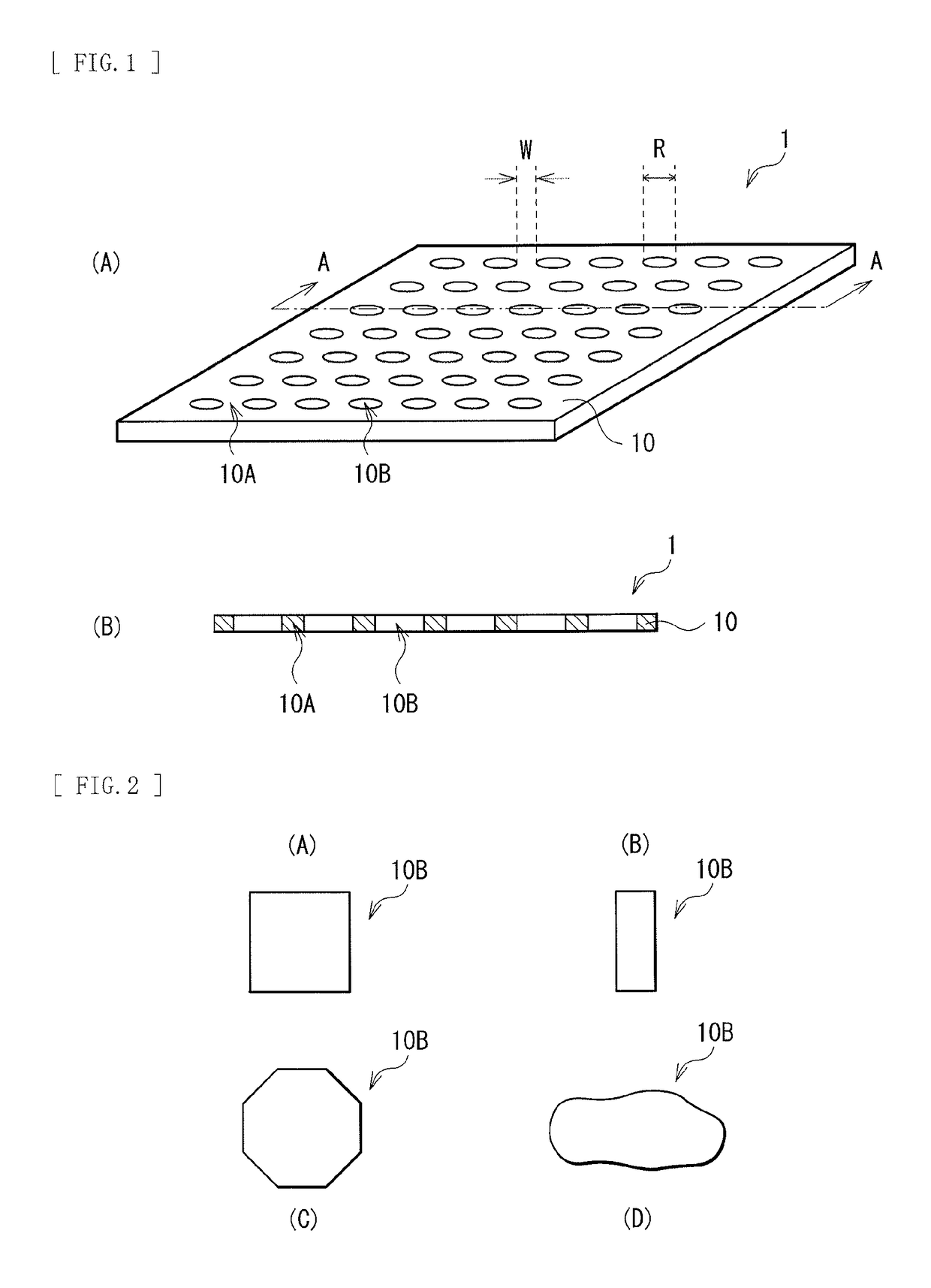
[0058]An example in which a notch is provided in place of an opening (FIG. 11)

[0059]An example in which a transparent conductive film is made of a plurality of conductive graphene sheets (FIG. 12 to FIG. 15)

[0060]An example in which a conductive graphene sheet is doped (FIG. 16)

[0061]An example in which an opening is filled with some kind of light transmissive material (FIG. 17, FIG. 19)

[0062]An example in which a conductive graphene sheet having no opening is provided (FIG. 18, FIG. 19)

3. Example (FIG. 20 to FIG. 30)

application examples (fig.31 to fig.38)

4. Application examples (FIG. 31 to FIG. 38)

1. Embodiment

[0063](Configuration)

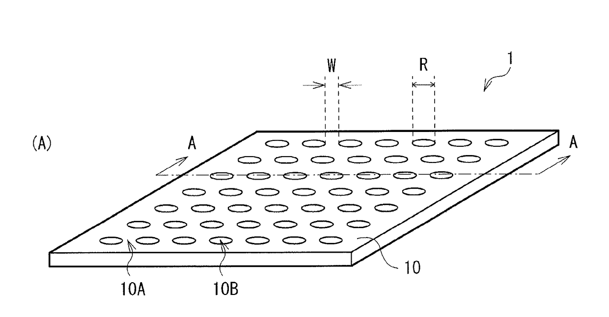
[0064]Part (A) of FIG. 1 illustrates an example of a top-surface configuration of a transparent conductive film 1 according to an embodiment. Part (B) of FIG. 1 illustrates an example of a cross-sectional configuration taken along a direction of arrows A-A in Part (A) of FIG. 1. This transparent conductive film 1 may include, for example, as illustrated in Part (B) in FIG. 1, a single-layered conductive graphene sheet 10. It is to be noted that the transparent conductive film 1 may include a highly-transparent layer, besides the conductive graphene sheet 10, and, for example, may include a glass substrate, a resin substrate, or the like supporting the conductive graphene sheet 10.

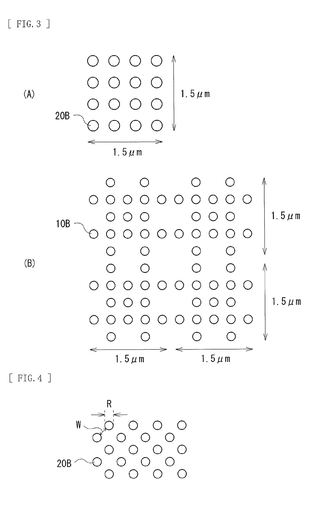
[0065]The conductive graphene sheet 10 may be configured to include, for example, as illustrated in Parts (A) and (B) of FIG. 1, a first region 10A, and a second region 10B surrounded by the first region 10A and having optical tra...

application examples

4. Application Examples

[0131]Next, application examples of the transparent conductive film 1 according to the embodiment and the modifications described above will be described. Various electronic apparatuses provided with the transparent conductive film 1 as an electrode will be described as the application examples of the transparent conductive film 1.

[0132](First Application Example)

[0133]FIG. 31 is a developed perspective view of a transparent heater 100 according to a first application example. The transparent heater 100 includes the transparent conductive film 1 as an electrode for heat generation. The transparent heater 100 includes an electrode 120 and the transparent conductive film 1 electrically connected to the electrode 120, between a transparent base material 110 and a transparent base material 130. The transparent base material 110 and the transparent base material 130 may be made of, for example, a glass substrate.

[0134]In the transparent heater 100, by a flow of a c...


PUM

PropertyMeasurementUnit
optical transmittanceaaaaaaaaaa
sheet resistanceaaaaaaaaaa
optical transmittanceaaaaaaaaaa

Abstract

There are provided a transparent conductive film, as well as a heater, a touch panel, a solar battery, an organic EL device, a liquid crystal device, and an electronic paper that are provided with the transparent conductive film, the transparent conductive film being capable of easing a decline in optical transmittance when graphene is laminated, and of achieving optical transmittance higher than an upper limit of optical transmittance of a single layer of graphene. The transparent conductive film includes a single-layered conductive graphene sheet. The single-layered conductive graphene sheet includes a first region and a second region, the first region being configured of graphene, and the second region being surrounded by the first region and having optical transmittance that is higher than optical transmittance of the first region.

Description

CROSS REFERENCES TO RELATED APPLICATIONS[0001]The present application is the national stage of International Application No. PCT / JP2012 / 057137, filed on Mar. 21, 2012, which claims the benefit under 35 U.S.C. §119 of Japanese Patent Application 2011-070355, filed on Mar. 28, 2011, and Japanese Patent Application 2012-009460, filed on Jan. 19, 2012.TECHNICAL FIELD[0002]The present technology relates to a transparent conductive film formed by laminating one or a plurality of graphenes, as well as a heater, a touch panel, a solar battery, an organic electroluminescence (EL) device, a liquid crystal device, and an electronic paper that are provided with the transparent conductive film.BACKGROUND ART[0003]A transparent conductive film is used for various devices such as a touch panel, a solar battery, an electronic paper, and an image sensor. Materials generally used as a transparent conductive film include indium tin oxide (ITO). An ITO film is a conductive material having extremely hig...

Claims


Application Information

Patent Timeline
Patent Type & Authority Patents(United States)
IPC IPC(8): B32B3/24H05B3/06B82Y30/00B82Y40/00B29D11/00H01L51/52G06F3/045G06F3/044H01L31/0224H01L51/44H05B3/14H01B5/00G02F1/1343G02F1/167G02F1/1333H01M14/00G02F1/1676
CPCH01B5/00B82Y30/00B82Y40/00C01B32/186G02F1/13439G06F3/044G06F3/045H01L31/022425H01L31/022466H01L51/442H01L51/5209H01L51/5215H01L51/5234H05B3/06H05B3/145B29D11/00788Y10T428/24802C01B2204/02G02B2207/121G02F1/13338G02F1/133382G02F2001/1676G02F2201/121G02F2202/16G02F2203/01G06F2203/04103H01M14/005H05B2214/04Y02E10/549Y10T428/24273Y10T428/24479G02F1/1676G06F3/0445G06F3/0444G06F3/0446H10K30/82H10K50/813H10K50/816H10K50/828G06F3/0448
Inventor SHIMIZU, KEISUKEKOBAYASHI, TOSHIYUKIKIMURA, NOZOMIIZUHA, KYOKO
Owner SONY CORP
Why Eureka
Try Eureka