
Methods and systems for reducing electrical disturb effects between thyristor memory cells using buried metal cathode lines

a technology of thyristor memory cells and metal cathode lines, applied in the direction of transistors, instruments, basic electric elements, etc., can solve the problems of reducing device performance and yield, and quadrupling the bit density

Active Publication Date: 2017-11-07
TC LAB INC
View PDF6 Cites 5 Cited by
  • Summary
  • Abstract
  • Description
  • Claims
  • Application Information

AI Technical Summary

Benefits of technology

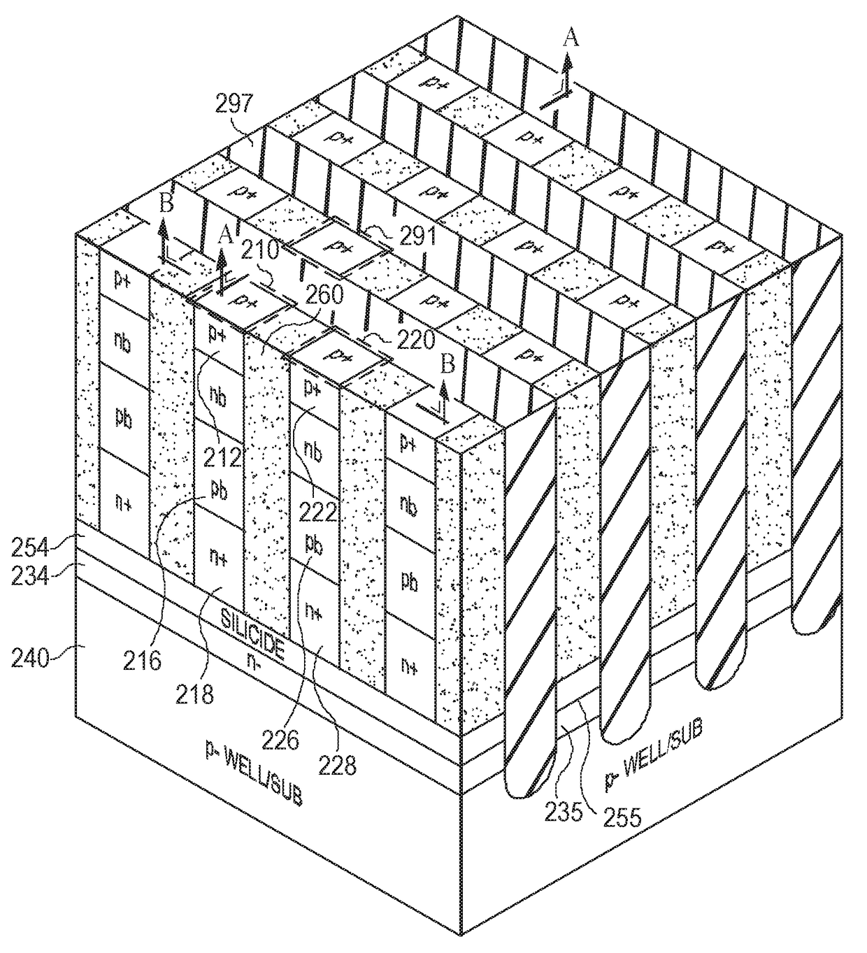
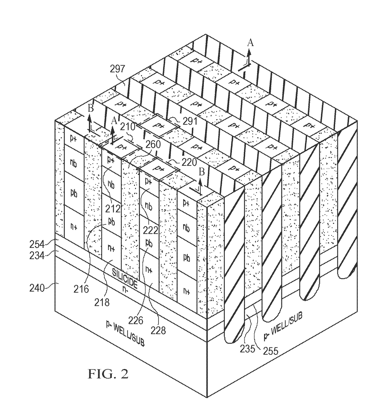
[0009]Vertical thyristors arranged in cross-point arrays offer a promising solution to the challenges described in the background of the disclosure. Methods and systems for reducing electrical disturb effects between thyristor memory cells in a memory array are provided herein.
[0010]In some embodiments, a cathode line connecting a first thyristor and second thyristor within a cross-point memory array is composed of a material that reduces a minority carrier lifetime within the cathode to reduce electrical disturb effects between the first thyristor and the second thyristor. The material may have a high conductivity in order to improve operating performance of the cross-point array of thyristor memory cells.
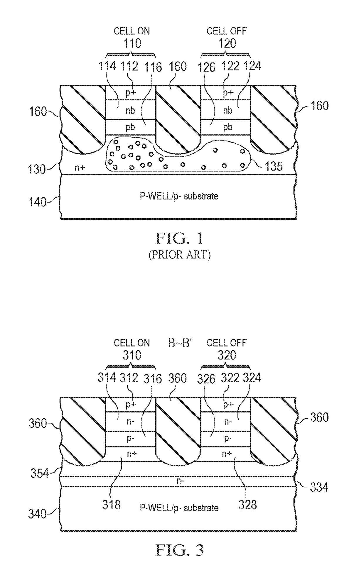
[0011]In some embodiments, a potential well may be formed within a cathode line connecting a first thyristor and a second thyristor within a cross-point memory array to confine minority carriers in order to reduce electrical disturb effects between the first thyristor and the second thyristor. The minority carriers may be collected from the potential well through an electrical contact to the potential well.
[0012]In some embodiments, a one-sided potential barrier may be formed in a cathode line connecting a first thyristor and a second thyristor within a cross-point memory array to divert minority carriers to a substrate contact in order to reduce electrical disturb effects between the first thyristor and the second thyristor.

Problems solved by technology

Bit density has quadrupled every three years by lithographical scaling and ever increasing process complexity.
Maintaining a sufficiently high capacitance value and low transistor leakage current has become a major problem for further scaling.
The technology has yet to solve its data retention issues, particularly at scaled dimensions.
The use of epitaxial or chemical vapor deposition (CVD) processed semiconductor layers at the backend of a standard CMOS process adds on thermal cycles and etch steps that may degrade performance and yield of devices already fabricated on the substrate earlier in a fabrication process (e.g., during front-end processing).
In addition, pnpn devices operated in the breakdown regime may pose challenges in process control and also power consumption.
Additionally, depending on the breakdown mechanism (e.g., tunneling breakdown, avalanching breakdown, etc.) operation in the breakdown regime may pose challenges to long-term reliability of switching and data retention of these memory devices due to physical degradation of component materials.

Method used


Image

  • Methods and systems for reducing electrical disturb effects between thyristor memory cells using buried metal cathode lines
  • Methods and systems for reducing electrical disturb effects between thyristor memory cells using buried metal cathode lines
  • Methods and systems for reducing electrical disturb effects between thyristor memory cells using buried metal cathode lines

Examples


Embodiment Construction

[0048]Vertical thyristors arranged in cross-point arrays offer a promising solution to the challenges described in the background of the disclosure. Advantages of thyristors include the ability to precisely tune operating characteristics (e.g., switching speed, static power consumption, dynamic power consumption, etc.) by tuning the geometry and composition of component layers of each thyristor cell. Vertical thyristors may be arranged as an array of minimum 4F2 cells, thereby minimizing cell area and reducing fabrication cost. Vertical thyristors may also be arranged in a stacked configuration to further increase the density of memory cells in a cross-point array.

[0049]Vertical thyristors may be arranged in a cross-point array of cells electrically isolated, for example, by trench isolation. As the isolation trenches in thyristor memories become narrower as the thyristor memories are scaled to smaller dimensions, minority carriers from ON cells can diffuse to neighboring OFF cells....


PUM


Abstract

Methods and systems for reducing electrical disturb effects between thyristor memory cells in a memory array are provided. Electrical disturb effects between cells are reduced by using a material having a reduced minority carrier lifetime as a cathode line that is embedded within the array. Disturb effects are also reduced by forming a potential well within a cathode line, or a one-sided potential barrier in a cathode line.

Description

CROSS REFERENCE TO RELATED APPLICATIONS[0001]This patent application claims priority from U.S. Provisional Patent Application No. 62 / 292,547, filed Feb. 8, 2016, and entitled “High Density Vertical Thyristor Memory Cell and Memory Array Using a Heterostructure Cathode”, U.S. Provisional Patent Application No. 62 / 294,239, filed Feb. 11, 2016, and entitled “Vertical Thyristor Memory Cell with Minority Carrier Lifetime Reduction Dopants”, and from U.S. Provisional Patent Application No. 62 / 294,270, filed Feb. 11, 2016, and entitled “Vertical Thyristor Memory Array with Metal Plug Wordlines”, and from U.S. Provisional Patent Application No. 62 / 300,015, filed Feb. 25, 2016, and entitled “Vertical Cross-Point Thyristor Memory Cell and Memory Array with Buried Metal Access Lines”.FIELD OF THE DISCLOSURE[0002]The disclosures described herein relate to semiconductor devices for information storage. The semiconductor devices can be used as volatile memories such as static random access memori...

Claims


Application Information

Patent Timeline
Patent Type & Authority Patents(United States)
IPC IPC(8): H01L29/74H01L21/8229H01L21/285H01L23/532H01L27/102H01L29/45
CPCH01L27/1027H01L21/28518H01L21/28525H01L21/28562H01L29/456H01L21/8229H01L23/53209H01L23/53242H01L21/28568G11C11/39H01L29/401H01L29/41716H10B99/00H01L27/0817H01L29/87H01L28/00H01L29/165H10B12/10H10B12/20H01L21/02271H01L21/221H01L21/32053H01L29/0642H01L29/16H01L29/66363H01L29/74H01L21/26513H01L29/0649H01L29/161H01L29/0839
Inventor LUAN, HARRYAXELRAD, VALERYCHENG, CHARLIE
Owner TC LAB INC
Learn More