
Super junction MOS bipolar transistor having drain gaps

a bipolar transistor and super junction technology, applied in the direction of permanent superconductor devices, electrical appliances, semiconductor devices, etc., can solve the problems of low switching loss, limited current density capability, and significant energy efficiency compromise in power switch device selection

Active Publication Date: 2020-03-03
D3 SEMICON
View PDF22 Cites 0 Cited by
  • Summary
  • Abstract
  • Description
  • Claims
  • Application Information

AI Technical Summary

Benefits of technology

This patent describes a new type of MOSFET (a type of semiconductor material) called the SJMOSBT that has faster switching speeds and reduced energy losses compared to an IGBT (a type of MOSFET). It achieves this by controlling the timing of current flow through the device. Standalone MOSFETs have slow switching speeds because they require a certain amount of time for minority carriers (which are electric current carriers) to recombine (recombine means to restore their original state). The SJMOSBT solves this problem by turning off the MOSFET current faster than it turns on, reducing the effective tail current (the electric current that lingers after the MOSFET has turned off). The SJMOSBT is also designed with alternating rows of heavily doped n-type and p-type dopants, which further reduces minority carrier lifetime and the need for additional processing steps. Overall, this technology allows for faster and more efficient switching than traditional MOSFETs and IGBTs.

Problems solved by technology

When designing power supplies and power conversion systems, significant compromises in energy efficiency must be made in power switch device selection due to the limitations imposed by the switching characteristics of the available switching elements.
A MOSFET is capable of fast switching and hence low switching losses, but has limited current-density capability, both of which are due to the majority-carrier nature of the device.
An IGBT, on the other hand, is a minority-carrier device which can achieve very high current-density but is limited in switching speed by minority-carrier-lifetime-induced tail current which results in extended turn-off time and thus higher switch-off energy loss compared to the MOSFET.

Method used


Image

  • Super junction MOS bipolar transistor having drain gaps
  • Super junction MOS bipolar transistor having drain gaps
  • Super junction MOS bipolar transistor having drain gaps

Examples


Embodiment Construction

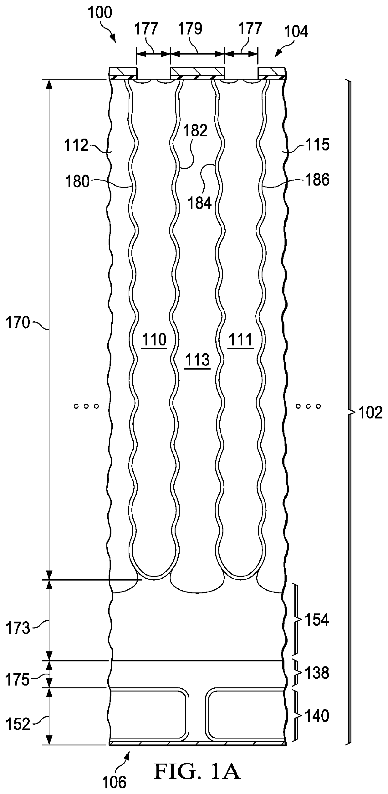
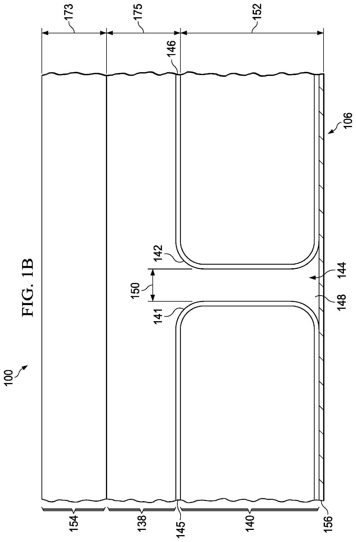
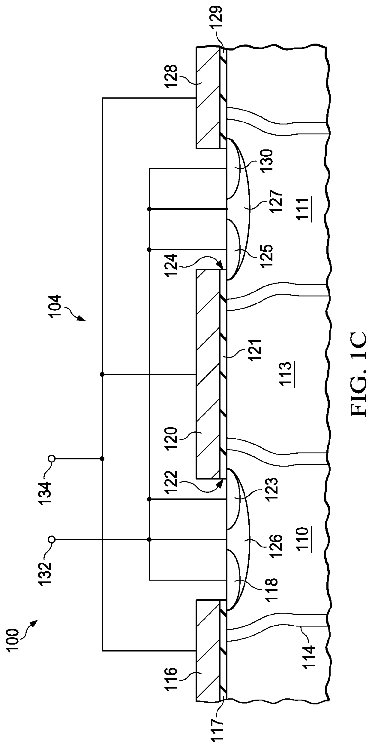
[0056]A preferred embodiment of the disclosed device is a vertically conducting FET-controlled power device with unipolar conduction at low current densities that transitions to bipolar conduction at high current densities. Bipolar conduction switches on after the unipolar conduction turns on. Unipolar conduction takes place in a highly-doped, charge-balanced drift region, thereby enabling faster switching due to the reduction in minority carrier tail current due to the enhanced recombination of minority carriers in the highly-doped charge-balance regions. Bipolar conduction switches off before the unipolar conduction switches off. These characteristics enable the device to switch faster because of a reduction in minority carrier tail current due to minority carriers starting recombination in the interval between bipolar conduction switch off and unipolar conduction switch off.

[0057]Referring to FIG. 1A, a partial cross-section of vertical semiconductor device 100 is shown. Vertical...


PUM

PropertyMeasurementUnit
widthaaaaaaaaaa
widthaaaaaaaaaa
depthaaaaaaaaaa

Abstract

Methods and designs are provided for a vertical power semiconductor switch having an IGBT-with-built-in-diode bottom-side structure combined with a SJMOS topside structure in such a way as to provide fast switching with low switching losses (MOSFET), low on-resistance at low currents (SJMOS), low on-resistance at high currents (IGBT), and high current-density capability (IGBT).

Description

CROSS REFERENCE TO RELATED APPLICATIONS[0001]This application claims priority to U.S. Provisional Application No. 62 / 468,726, filed Mar. 8, 2017, which is incorporated herein by reference in its entirety to provide continuity of disclosure.TECHNICAL FIELD OF THE INVENTION[0002]This invention relates generally to increasing the energy efficiency, reducing the switching time, and increasing the current-carrying capability of a power semiconductor switch by optimal combination and design of a merged SuperJunction MOSFET-IGBT transistor. In particular, this invention details methods and designs for a vertical power semiconductor switch having an IGBT-with-built-in-diode bottom-side structure combined with a SJMOS topside structure in such a way as to provide fast switching with low switching losses (MOSFET), low on-resistance at low currents (SJMOS), low on-resistance at high currents (IGBT), and high current-density capability (IGBT).BACKGROUND OF THE INVENTION[0003]When designing powe...

Claims


Application Information

Patent Timeline
Patent Type & Authority Patents(United States)
IPC IPC(8): H01L29/73H01L29/08H01L29/06H01L29/78H01L29/66H01L39/22H01L39/14H01L29/739H01L21/02H10N60/20
CPCH01L21/02016H01L29/0619H01L29/0696H01L29/0634H01L29/7396H01L29/7802H01L29/66333H01L29/7395H01L39/145H01L29/0834H01L39/228H10N60/128H10N60/205
Inventor HARRINGTON, III, THOMAS E.QU, ZHIJUN
Owner D3 SEMICON
Learn More