Semiconductor device and method for producing the same

a semiconductor and device technology, applied in semiconductor devices, diodes, electrical devices, etc., can solve problems such as misfit dislocation, and achieve the effect of shortening the carrier lifetime and high resistan

Inactive Publication Date: 2013-08-22
NGK INSULATORS LTD
View PDF1 Cites 0 Cited by
  • Summary
  • Abstract
  • Description
  • Claims
  • Application Information

AI Technical Summary

Benefits of technology

[0010]An object of the present invention is to further develop the concept of the semiconductor device described in Japanese Laid-Open Patent Publication No. 2005-285955, thereby providing a semiconductor device having a preferred structure containing an active high-resistance layer (AIL), which exhibits high resistance and is effective at shortening the carrier lifetime. The present invention also provides a method for producing the aforementioned semiconductor device.
[0012]The distances Da and Db are selected based on the above condition. Consequently, when the anode-cathode state is converted from a forward bias state to a reverse bias state, the delay time can be shortened due to a minority-carrier storage effect. Furthermore, a gate-cathode reverse voltage can be prevented from rising rapidly in the reverse bias state, a gate-cathode reverse current can be reduced in order to slow a change (slope di / dt) in returning to the steady state, and gate-cathode fracturing can be prevented.
[0026]During the process of disposing the epitaxial layer on the semiconductor substrate, the active high-resistance semiconductor segment is formed, wherein the active high-resistance semiconductor segment is doped with a high concentration of a first conductive type impurity and a high concentration of a second conductive type impurity. Thus, the majority carrier lifetime and the minority carrier lifetime can effectively be shortened.
[0028]In such a production method, an active high-resistance semiconductor segment, which has high resistance and is effective at shortening the carrier lifetime, can easily be formed between the embedded gate segments and the cathode segment. Particularly, in the first step, a portion, which ultimately will be converted into the active high-resistance semiconductor segment, can be protected by the photomask, whereby the portion can be prevented from becoming scratched. Although the impurity layer also is formed on the upper surface of the photomask in the second step, the portion, which will be converted into the active high-resistance semiconductor segment, can be protected by the photomask, the portion can be maintained in a crystalline form, and the portion can be prevented from becoming contaminated with impurities (metal). Furthermore, the concentration of impurities in the impurity layer can be controlled by removing the superficial layer in the third step, so that the active high-resistance semiconductor layer formed in the following fifth step can suitably be used as the intrinsic semiconductor segment. In addition, the production method is capable of easily producing a semiconductor device satisfying the condition Db≦(⅓)×Da, in which Da represents a distance between the top surface of the cathode segment and an end of the embedded gate segments facing the anode segment, and Db represents a distance between a highest-impurity concentration portion in the embedded gate segments and an end of the cathode segment facing the anode segment.
[0029]As described above, in the semiconductor device of the present invention, when the anode-cathode state is converted from a forward bias state to a reverse bias state, due to a minority-carrier storage effect, the delay time can be shortened. Furthermore, a gate-cathode reverse voltage can be prevented from rising rapidly in a reverse bias state, and a gate-cathode reverse current can be reduced in order to slow a change (slope di / dt) in returning to a steady state condition, whereby fracturing of the gate-cathode can be prevented.
[0030]In the semiconductor device production method of the invention, an active high-resistance semiconductor segment, which has high resistance and is effective at shortening the carrier lifetime, can easily be formed between the embedded gate segments and the cathode segment. In addition, the production method is capable of easily producing a semiconductor device that satisfies the condition Db≦(⅓)×Da, in which Da represents a distance between the top surface of the cathode segment and an end of the embedded gate segments facing the anode segment, and Db represents a distance between a highest-impurity concentration portion in the embedded gate segments and an end of the cathode segment facing the anode segment.

Problems solved by technology

In the event that the high-resistance semiconductor layer is doped with an impurity, due to different lattice constants between the impurity atoms and the layer, the crystal is likely to become strained, thereby causing dislocations such as a misfit dislocation.

Method used


Image

  • Semiconductor device and method for producing the same
  • Semiconductor device and method for producing the same
  • Semiconductor device and method for producing the same

Examples


first example

[0076]In a First Example, in each of semiconductor devices according to the Reference Example and Examples 1 to 9, a reverse voltage, which was generated by converting the forward bias state into a reverse bias state, was measured. The measured reverse voltage was represented by an absolute value of the peak value Vp throughout all of the examples. More specifically, a rated current of 30 A was applied as a forward current IF (see FIG. 4), followed by applying a reverse bias, and the reverse voltage Vp was measured. Characteristic values and measurement results according to the Reference Example and Examples 1 to 9 are shown in Table 1. It should also be noted, in the Reference Example and in Examples 1 to 9, each of the AILs 36 was doped with gold (Au) at 50 atm.

Reference Example

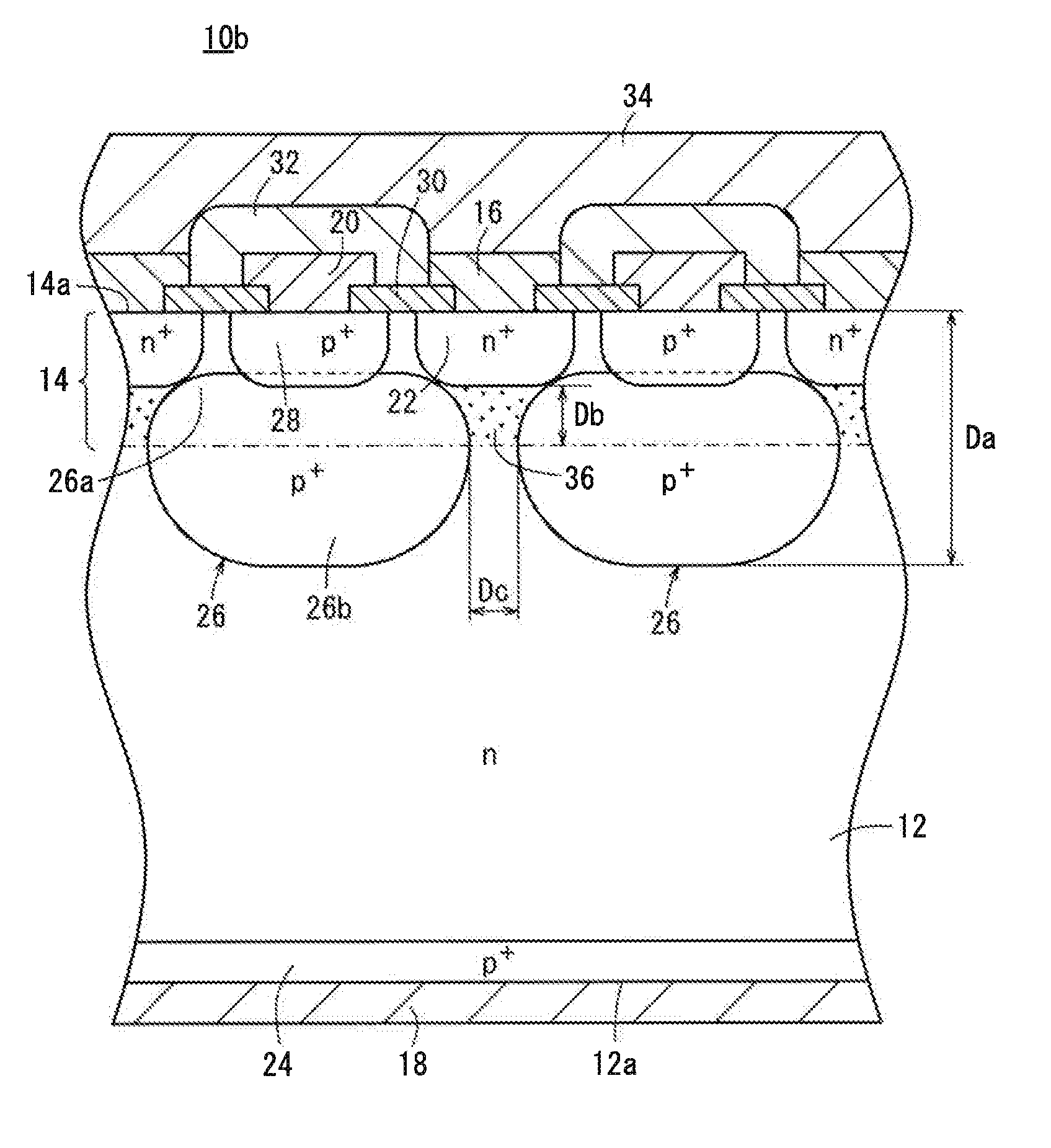
[0077]In the semiconductor device according to the Reference Example, the distance Da was 18 μm, the distance Db was 9 μm, and the distances Da and Db satisfied the relationship Db / Da=½.

example 1

[0078]In the semiconductor device according to Example 1, the distance Da was 6 μm, the distance Db was 2.0 μm, and the distances Da and Db satisfied the relationship Db / Da=⅓.

examples 2 to 9

[0079]In each of the semiconductor devices according to Examples 2, 3, 4, 5, 6, 7, 8, and 9, the distance Da was 6 μm, the distance Db was 1.5, 1.3, 1.1, 1.0, 0.9, 0.7, 0.6, or 0.5 μm, respectively, and the distances Da and Db satisfied the relationship Db / Da=¼, 13 / 60, 11 / 60, ⅙, 3 / 20, 7 / 60, 1 / 10, or 1 / 12, respectively.

TABLE 1DistanceDistanceReverse voltageDa [μm]Db [μm]Db / DaVp [kV]Reference Example18.09.01 / 23.0Example 16.02.01 / 32.4Example 26.01.51 / 42.2Example 36.01.313 / 602.0Example 46.01.111 / 601.9Example 56.01.01 / 61.8Example 66.00.9 3 / 201.8Example 76.00.7 7 / 602.0Example 86.00.6 1 / 102.2Example 96.00.5 1 / 122.5

[0080]As shown in Table 1, when a rated current of 30 A was applied as the forward current followed by application of the reverse bias, the semiconductor device according to the Reference Example exhibited a reverse voltage of 3 kV. On the other hand, the semiconductor devices according to Examples 1 to 9 exhibited reverse voltages, which were lower than that of the Reference Exa...


PUM

PropertyMeasurementUnit
distanceaaaaaaaaaa
distanceaaaaaaaaaa
distanceaaaaaaaaaa

Abstract

A semiconductor device satisfies the condition Db≦(⅓)×Da, in which Da represents a distance between a top surface of a cathode segment and an end of an embedded gate segment facing an anode segment, and Db represents a distance between a highest-impurity concentration portion in the embedded gate segment and an end of the cathode segment facing the anode segment.

Description

CROSS-REFERENCE TO RELATED APPLICATION[0001]This application is based upon and claims the benefit of priority from Japanese Patent Application No. 2012-031722 filed on Feb. 16, 2012, the contents of which are incorporated herein by reference.BACKGROUND OF THE INVENTION[0002]1. Field of the Invention[0003]The present invention relates to a semiconductor device suitable for use in a static induction thyristor, a GTO thyristor, etc., and to a method for producing the same. More specifically, the present invention relates to a semiconductor device containing an active high-resistance semiconductor layer (active intrinsic layer AIL), which exhibits high resistance and is effective at shortening the carrier lifetime, as well as to a method for producing the same.[0004]2. Description of the Related Art[0005]Static induction thyristors and static induction transistors have been developed and used practically as power semiconductor devices. For improving speed, lifetime control of such semic...

Claims


Application Information

Patent Timeline
Patent Type & Authority Applications(United States)
IPC IPC(8): H01L29/739H01L29/66
CPCH01L29/66333H01L29/7395H01L21/2254H01L29/66356H01L29/7392H01L29/36H01L21/2252H01L21/2205
Inventor SHIMIZU, NAOHIROYOKOI, SHOJI
Owner NGK INSULATORS LTD
Why Eureka
Try Eureka