

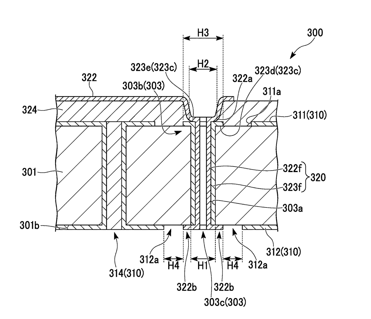
Mode converter between a plane circuit and a substrate waveguide including a pin having a land and an anti-pad
a plane circuit and waveguide technology, applied in waveguides, semiconductor devices, electrical devices, etc., can solve the problems of difficult to realize the optimal length of the pin, the thickness of the substrate to be stacked cannot be determined individually, and the impedance adjustment is not easy, so as to improve the efficiency of the operation process, improve the operation reliability and yield, and confirm the positional relationship. the effect of easy operation
- Summary
- Abstract
- Description
- Claims
- Application Information
AI Technical Summary
Benefits of technology
Problems solved by technology
Method used
Image

Examples
example 1
[0156]Example 1 using the above mode converter is described. Regarding each of a case that uses a mode converter according to the present exemplary embodiment (FIG. 5) and a case that uses a mode converter according to prior art (FIG. 35), simulations were performed on components to be reflected (i.e., reflection loss) of the signals which were transmitted to pins from the plane circuit (high-frequency transmission line). The software HFSS for a three-dimensional electromagnetic-field analysis was used in the simulation, and both in the present exemplary embodiment and in prior art, the thickness of the first substrate was 850 μm. The simulation results are shown in the graph of FIG. 24. In the mode converter of the present exemplary embodiment, the size of the other anti-pad of the first substrate was 100 μm.
[0157]The horizontal axis of the graph represents the frequency in GHz of the signal to be propagated to the pin from the transmission circuit, and the vertical axis represents...
example 2
[0158]Example 2 using the above mode converter is described. Regarding each of a case that uses a mode converter according to the present exemplary embodiment (FIG. 5) and a case that uses a mode converter according to prior art (FIG. 35), simulations were performed on components to be leaked from an opening portion at another main surface 301b of the first substrate (i.e., transmission loss) of the signals which were transmitted from the plane circuit. The software HFSS for a three-dimensional electromagnetic-field analysis was used in the simulation, and both in the present exemplary embodiment and in prior art, the thickness of the first substrate was 850 μm. The simulation results are shown in the graph of FIG. 25. In the mode converter of the present exemplary embodiment, the size of the other anti-pad of the first substrate was 100 μm.
[0159]The horizontal axis of the graph represents the frequency in GHz of the signal to be propagated to the pin from the transmission circuit, ...
example 3
[0160]Example 3 using the above mode converter is described. Regarding each of a case that uses a mode converter according to the present exemplary embodiment (FIG. 5) and a case that uses a mode converter according to prior art (FIG. 35), simulations were performed on an electric field distribution generated inside the first substrate when the mode converter is operated. The software HFSS for a three-dimensional electromagnetic-field analysis was used in the simulation, and both in the present exemplary embodiment and in prior art, the thickness of the first substrate was 850 μm. The simulation results of the prior art and the present exemplary embodiment are respectively shown FIG. 26A and FIG. 26B. However, the electric field distribution is varied over time in practice, and therefore, these graphs show the electric field distribution at a certain moment.
[0161]In order to show the electric field distribution generated in the inside of the mode converter 300, components other than...
PUM
 Abstract
Description
Claims
Application Information