Methods for preparation of concentrated graphene ink compositions and related composite materials
a graphene ink composition and composite material technology, applied in the field of concentrated graphene ink compositions and related composite materials, can solve the problems of significant structural and chemical defects, poor electrical conductivity of reduced go flakes, and deficiency, so as to achieve the effect of substantially maintaining the morphology of printed materials, electrical performance and mechanical properties
- Summary
- Abstract
- Description
- Claims
- Application Information
AI Technical Summary
Benefits of technology
Problems solved by technology
Method used
Image
Examples
example 2
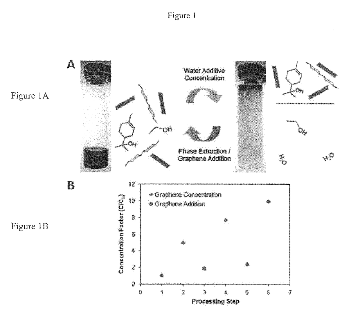
[0067]Graphene Concentration Via Iterative Solvent Exchange. To ensure proper hydrophobic phase separation, water, in excess of four times the volume of the starting graphene solution, is added. A brief sonication step, of approximately 1 min, is also performed after each graphene concentration and graphene addition step to facilitate phase separation and solution mixing.
example 3
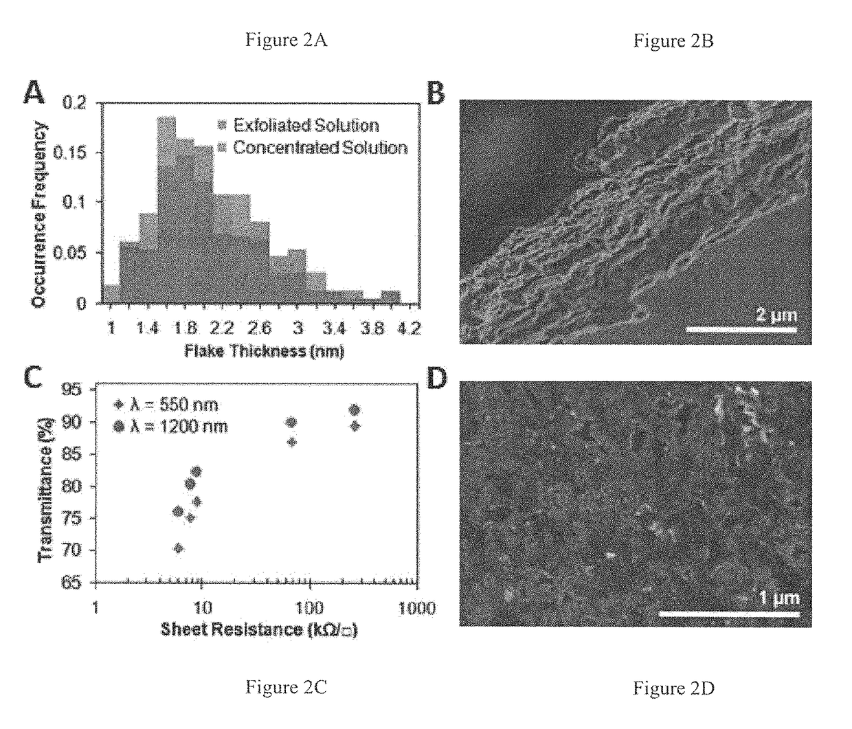
[0068]SiO2 Graphene Deposition. Graphene flakes from both the sedimented graphene solution and third-iteration concentrated graphene solution were deposited onto 100 nm thick oxide silicon wafers for imaging. The wafers were first submerged in 2.5 mM 3-aminopropyl triethoxysilane aqueous solution to functionalize the surface with a hydrophobic self-assembling monolayer for 30 min. The substrates were then rinsed with water and dried under a stream of N2. Both graphene solutions were then diluted to approximately 0.02 mg / mL in ethanol after which a drop of each was placed onto the functionalized wafers for 10 min. The drops were then blown off under a stream of N2, and the wafer was rinsed with water. To remove the residual EC, the wafers were annealed for 20 min at 400° C. in air.
example 4
[0069]Atomic Force Microscopy Thickness Measurements. All atomic force microscopy (AFM) images were obtained using a Thermo Microscopes Autoprobe CP-Research AFM in tapping mode using cantilever B on MikroMasch NSC NSC36 / Cr—AuBS probes. 2 μm×2 μm images were collected using identical scanning parameters. Flake thicknesses were determined using line-scan thickness profiles across flakes larger than 5,000 nm2 while avoiding regions where EC residues were present. (FIG. 3) 146 flakes were analyzed on the wafer deposited with the sedimented graphene solution, and 156 flakes were analyzed for the wafer deposited with the third-iteration concentrated graphene solution.
PUM
| Property | Measurement | Unit |
|---|---|---|
| solubility | aaaaa | aaaaa |
| concentrations | aaaaa | aaaaa |
| concentrations | aaaaa | aaaaa |
Abstract
Description
Claims
Application Information


