Integrated silicon-OLED display and touch sensor panel

a touch sensor panel and integrated technology, applied in the field of display and touch sensor panel, can solve the problems of damage to the oled stack, poor manufacturing yield, and inability to manufacture, and achieve the effects of wide viewing angle, higher contrast ratio, and improved manufacturing efficiency

Active Publication Date: 2017-12-05
APPLE INC
View PDF41 Cites 43 Cited by
  • Summary
  • Abstract
  • Description
  • Claims
  • Application Information

AI Technical Summary

Benefits of technology

[0004]This relates to integrated Silicon-OLED display and touch sensor panel stackup configurations that can be used in portable electronic devices such as media players, mobile telephones, and tablet computing devices. Stackup configurations can include a Silicon substrate, an array of transistors, one or more metallization layers, one or more vias, an OLED stack, color filters, touch sensors, and additional components and circuitry. Forming the OLED stack and touch sensors on a Silicon substrate can allow for an extremely high number of pixels per inch. With a high number of pixels per inch, the OLED subpixels can be arranged side-by-side with the touch sensors leading to portable electronic devices that are thinner and lighter. Arranging the OLED subpixels side-by-side with the touch sensors can also lead to a wider viewing angle display with a higher contrast ratio, higher brightness, and more vibrant colors without compromising touch sensitivity.
[0005]Due to the higher number of pixels per inch, the stackup configurations can also include one or more additional components such as electrostatic discharge devices, switches, near-field imagers, near-infrared emitters, and near-infrared detectors. The additional components can improve the functionality of the device by consuming less power, enhancing touch sensitivity, and enhancing fingerprint detection capabilities. In some examples, the integrated Silicon-OLED display and touch sensor panel can be coupled with one or more fiber optic magnifiers to achieve a portable electronic device with extended touch and display capability.

Problems solved by technology

However, both techniques can include high temperature or high pressure processes that can damage the OLED stack.
Furthermore, stacking the touch sensors and any routing circuitry for the touch sensors on the OLED stack can lead to portable electronic devices with unacceptable thicknesses.
Additionally, formation of the OLED stack on a glass or plastic substrate can lead to poor manufacturing yields, high process variations, and poor transistor / wiring performance.

Method used


Image

  • Integrated silicon-OLED display and touch sensor panel
  • Integrated silicon-OLED display and touch sensor panel
  • Integrated silicon-OLED display and touch sensor panel

Examples


Embodiment Construction

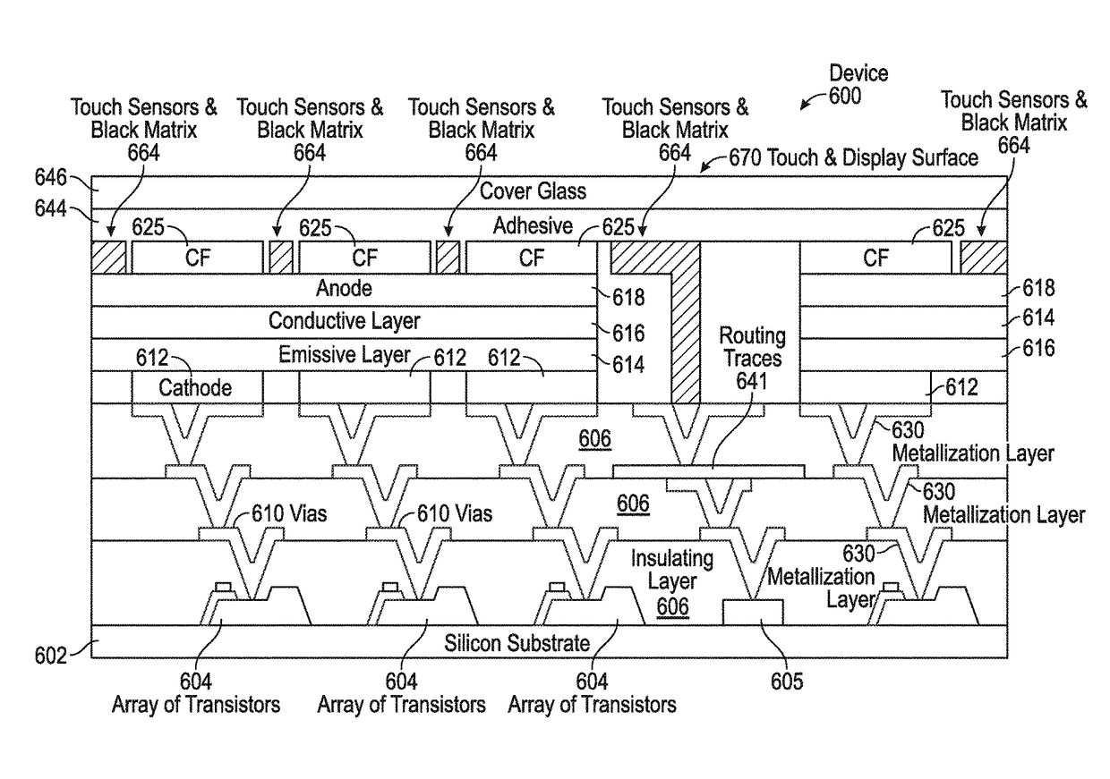
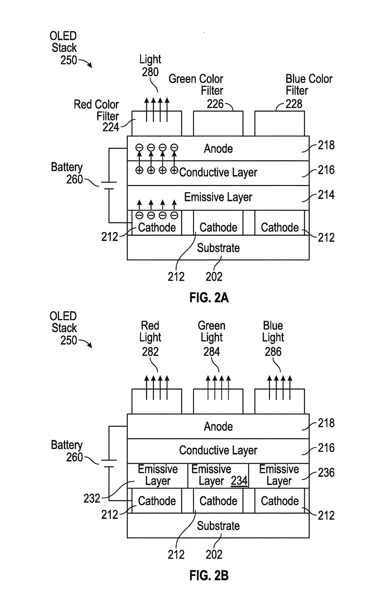
[0039]In the following description of examples, reference is made to the accompanying drawings which form a part hereof, and in which it is shown by way of illustration specific examples that can be practiced. It is to be understood that other examples can be used and structural changes can be made without departing from the scope of the disclosed examples.

[0040]Various techniques and process flow steps will be described in detail with reference to examples as illustrated in the accompanying drawings. In the following description, numerous specific details are set forth in order to provide a thorough understanding of one or more aspects and / or features described or referenced herein. It will be apparent, however, to one skilled in the art, that one or more aspects and / or features described or referenced herein may be practiced without some or all of these specific details. In other instances, well-known process steps and / or structures have not been described in detail in order to no...


PUM


Abstract

An integrated Silicon-OLED display and touch sensor panel is disclosed. The integrated Silicon-OLED display and touch sensor panel can include a Silicon substrate, an array of transistors, one or more metallization layers, one or more vias, an OLED stack, color filters, touch sensors, and additional components and circuitry. Additional components and circuitry can include an electrostatic discharge device, a light shielding, a switching matrix, one or more photodiodes, a near-infrared detector and near-infrared color filters. The integrated Silicon-OLED display and touch sensor panel can be further configured for near-field imaging, optically-assisted touch, and fingerprint detection. In some examples, a plurality of touch sensors and / or display pixels can be grouped into clusters, and the clusters can be coupled to a switching matrix for dynamic change of touch and / or display granularity.

Description

FIELD OF THE DISCLOSURE[0001]This relates generally to a display and touch sensor panel and, more particularly, to an integrated Silicon-OLED display and touch sensor panel.BACKGROUND OF THE DISCLOSURE[0002]Many types of input devices are presently available for performing operations in a computing system, such as buttons or keys, mice, trackballs, joysticks, touch sensor panels, touch screens and the like. Touch screens, in particular, are becoming increasingly popular because of their ease and versatility of operation as well as their declining price. Touch screens can include a touch sensor panel, which can be a clear panel with a touch-sensitive surface, and a display device positioned partially or fully behind the panel so that the touch-sensitive surface can cover at least a portion of the viewable area of the display device. The display device can include technologies such as liquid crystal displays (LCDs), organic light emitting diode (OLED) displays, etc. OLEDs, for example...

Claims


Application Information

Patent Timeline
Patent Type & Authority Patents(United States)
IPC IPC(8): G06F3/044H01L27/32G06F3/041G06F3/042G06K9/00
CPCG06F3/0421G06F3/042G06F3/044G06K9/0002H01L27/323G06F3/0412G06F2203/04106G06F2203/04103G06F3/0446G06F3/04164G06F3/0443G06V40/1306H10K59/38H10K59/40H10K59/121H10K59/131H10K50/86G06F3/0445H10K59/65
Inventor NHO, HYUNWOO HENRYBAE, HOPILYAO, WEIJUNLI, YINGXUANAL-DAHLE, AHMAD
Owner APPLE INC
Why Eureka
Try Eureka