Organic light emitting diode display

a light-emitting diode and organic technology, applied in the direction of diodes, semiconductor devices, electrical devices, etc., can solve the problems of destructive interference between external light reflected by the first metal layer and external light reflected by the second metal layer, so as to increase light efficiency, reduce the thickness of the display, and not deteriorate contrast and visibility.

Active Publication Date: 2018-01-02
SAMSUNG DISPLAY CO LTD
View PDF20 Cites 5 Cited by
  • Summary
  • Abstract
  • Description
  • Claims
  • Application Information

AI Technical Summary

Benefits of technology

[0010]Embodiments of the present invention provide for an organic light emitting diode display. Further embodiments provide for an organic light emitting diode display capable of preventing contrast and visibility from being deteriorated by reflection of external light.
[0027]Embodiments of the present invention provide for an organic light emitting diode display where, when a user uses the display outdoors, a vivid image is displayed and contrast and visibility are not deteriorated. Further embodiments provide for an organic light emitting diode display where a light blocking layer is used instead of a polarizing plate, such that light emitted from the organic light emitting layer may be appropriately transferred to the outside, thereby making it possible to increase light efficiency. In addition, by removing the polarizing plate, the entire thickness of the display may be decreased.
[0028]Still further embodiments provide for an organic light emitting diode display where the light blocking layer has conductivity and contacts a pixel electrode, such that resistance of the pixel electrode may be decreased. This may make it possible to prevent luminance from being non-uniform due to a voltage drop (IR-drop) generated in the organic light emitting diode display.

Problems solved by technology

The first and second metal layers may be configured so that external light reflected by the first metal layer and external light reflected by the second metal layer destructively interfere with each other.

Method used


Image

  • Organic light emitting diode display
  • Organic light emitting diode display
  • Organic light emitting diode display

Examples


first embodiment

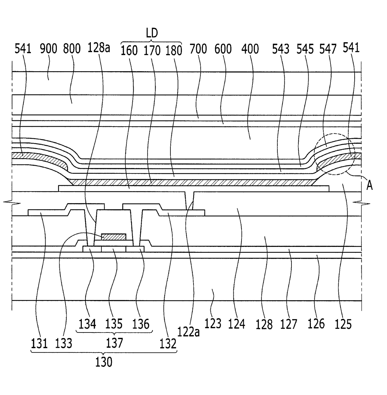
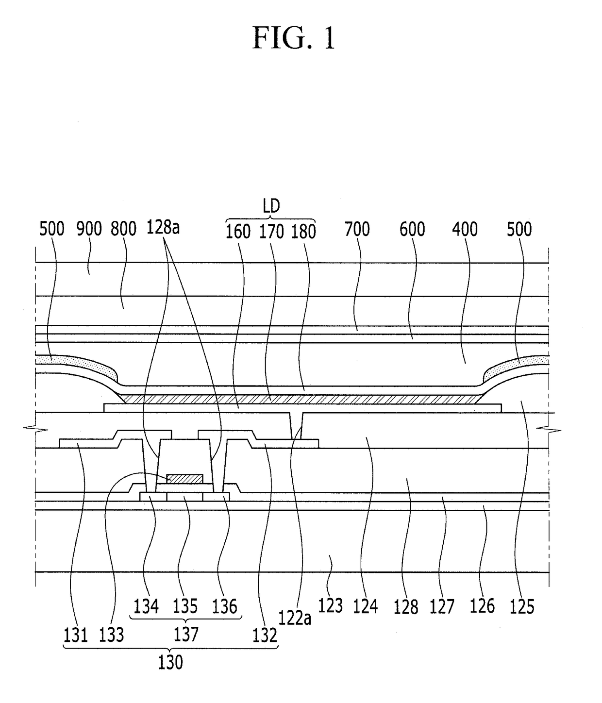
[0041]Hereinafter, an organic light emitting diode display will be described with reference to FIGS. 1 and 2.

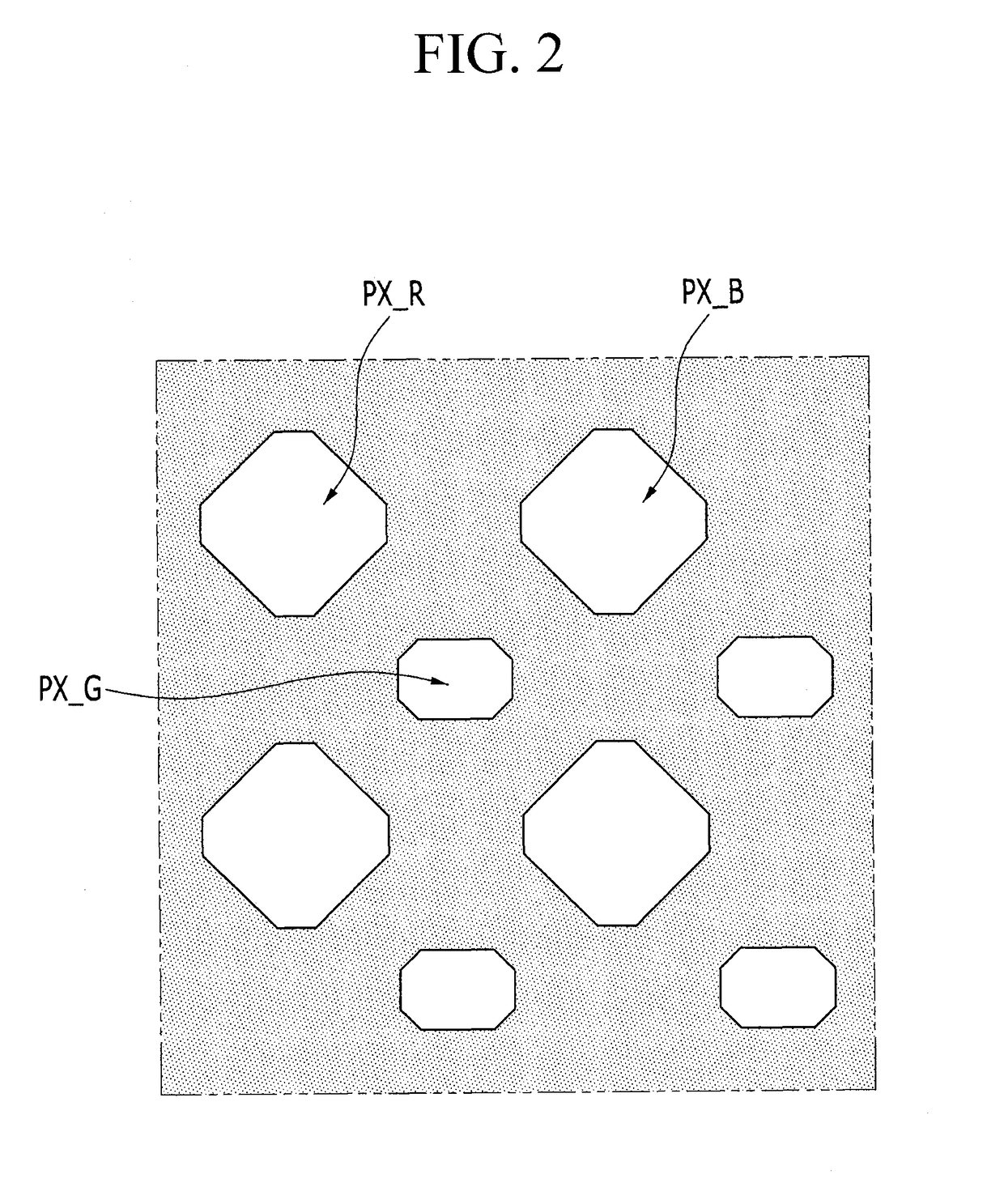
[0042]FIG. 1 is a schematic cross-sectional view of the organic light emitting diode display. FIG. 2 is a plan view of the organic light emitting diode display in which a light blocking layer is disposed.

[0043]Referring to FIG. 1, the organic light emitting diode display includes a substrate 123, a thin film transistor 130, a pixel defining layer 125, a first electrode 160, an organic light emitting layer 170, a second electrode 180, and a light blocking layer 500.

[0044]The substrate 123 may be formed as an insulating substrate made of glass, quartz, ceramic, plastic, or the like. However, the present invention is not limited thereto, and in other embodiments, the substrate 123 may be made of an insulating material having flexibility such as one or more of polyimide (PI), polyetherimide (PEI), polyethylene terephthalate (PET), polycarbonate (PC), polymethylmethacrylate (PMMA...

second embodiment

[0072]Hereinafter, an organic light emitting diode display will be described with reference to FIG. 3. Detailed descriptions of the same or similar components to those of FIG. 1 may not be repeated.

[0073]FIG. 3 is a schematic cross-sectional view of the organic light emitting diode display. Referring to the organic light emitting diode display of FIG. 3, a color filter layer 530 contacting the second electrode 180 may be disposed at a position corresponding to the pixel area.

[0074]In the embodiment of FIG. 1, the light blocking layer 500 is disposed on the second electrode 180, exposing the second electrode 180 at positions corresponding to the pixel area.

[0075]In FIG. 3, the color filter layer 530 is disposed in the exposure region of the light blocking layer 500. The color filter layer 530 contacts the second electrode 180. In further detail, the color filter layer 530 contacts the second electrode 180 while filling the exposure region of the light blocking layer 500.

[0076]The co...

third embodiment

[0082]Hereinafter, an organic light emitting diode display will be described with reference to FIG. 4 in addition to FIGS. 1 and 3 described above. Detailed descriptions of the same or similar components to those of the above-mentioned displays may not be repeated.

[0083]FIG. 4 is a schematic cross-sectional view of the organic light emitting diode display. Referring to the organic light emitting diode display of FIG. 4, an encapsulation layer 400 is disposed on a second electrode 180 and a light blocking layer 500, unlike the organic light emitting diode display of FIG. 3. In FIG. 4, a color filter layer contacting the second electrode 180 is not disposed on the second electrode 180 at a position corresponding to a pixel area. In other respects, the organic light emitting diode display of FIG. 4 has substantially the same configuration from the substrate 123 to the encapsulation layer 400 of the organic light emitting diode display of FIGS. 1 and 3.

[0084]In the organic light emitti...


PUM


Abstract

An organic light emitting diode display includes a substrate, a thin film transistor on the substrate, a first electrode on and connected to the thin film transistor, a pixel defining layer on the first electrode and defining a pixel area, an organic light emitting layer on the first electrode and contacting the first electrode exposed in the pixel area, a second electrode on the organic light emitting layer, and a light blocking layer on the second electrode and exposing the second electrode at a position corresponding to the pixel area. The light blocking layer may include a first metal layer on the second electrode and exposing the second electrode at a position corresponding to the pixel area, a first intermediate layer covering the first metal layer, a second metal layer covering the first intermediate layer, and a second intermediate layer covering the second metal layer.

Description

CROSS-REFERENCE TO RELATED APPLICATION[0001]This application claims priority to and the benefit of Korean Patent Application No. 10-2015-0062084, filed in the Korean Intellectual Property Office on Apr. 30, 2015, the entire content of which is incorporated herein by reference.BACKGROUND[0002]1. Field[0003]Aspects of embodiments of the present invention relate to an organic light emitting diode display.[0004]2. Description of the Related Art[0005]An organic light emitting element of an organic light emitting diode display includes two electrodes and an organic light emitting layer positioned therebetween. Electrons injected from a cathode, which is one of the electrodes, and holes injected from an anode, which is another one of the electrodes, are combined with each other in the organic light emitting layer to form excitons. The formed excitons emit energy, such that the organic light emitting element emits light.[0006]The organic light emitting diode display includes a plurality of ...

Claims


Application Information

Patent Timeline
Patent Type & Authority Patents(United States)
IPC IPC(8): H01L27/32H01L51/52
CPCH01L27/3272H01L27/322H01L27/3246H01L51/5284H01L51/5281H01L51/5253H01L27/323H10K59/38H10K59/40H10K59/126H10K59/122H10K50/86H10K50/865H10K50/844
Inventor KANG, SEOCK HWANPARK, WON SANGLIM, JAE IKCHOI, JIN-WOO
Owner SAMSUNG DISPLAY CO LTD
Why Eureka
Try Eureka