Circuit board structure with chips embedded therein and manufacturing method thereof

Active Publication Date: 2018-01-02
BOARDTEK ELECTRONICS CORP
View PDF2 Cites 6 Cited by
  • Summary
  • Abstract
  • Description
  • Claims
  • Application Information

AI Technical Summary

Benefits of technology

[0003]The instant disclosure provides a circuit board structure with chips embedded therein and a manufac

Problems solved by technology

However, the power chip (e.g., high-power chip) cannot be individually tested, so the power chip needs to be embedded in the conventional circuit board structure for using a plurality of conductive lines of the conventional circuit board structure to test the power chip.
Specifically, the conductive lines are formed by filling conductive material into a plurality of thru-holes of the conventional circuit b

Method used


Image

  • Circuit board structure with chips embedded therein and manufacturing method thereof
  • Circuit board structure with chips embedded therein and manufacturing method thereof
  • Circuit board structure with chips embedded therein and manufacturing method thereof

Examples


first embodiment

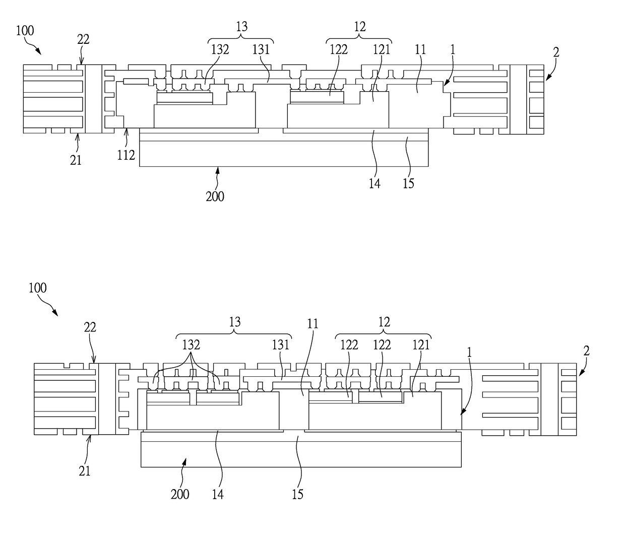
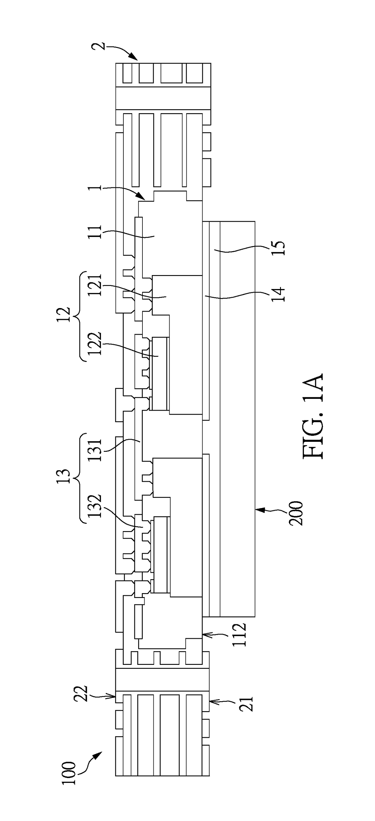
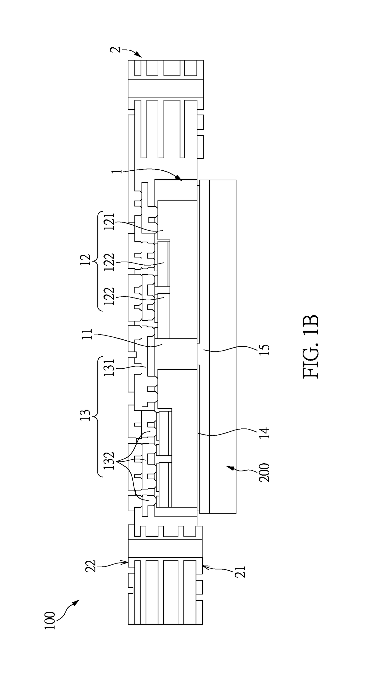
[0034]Please refer to FIGS. 1A through 6, which show a first embodiment of the instant disclosure. References are hereunder made to the detailed descriptions and appended drawings in connection with the instant invention. However, the appended drawings are merely shown for exemplary purposes, rather than being used to restrict the scope of the instant invention.

[0035]Please refer to FIG. 1A, which shows a circuit board structure 100 with chips embedded therein, in particular to a circuit board structure 100 with high-power chips embedded therein, but the instant disclosure is not limited thereto. The circuit board structure 100 includes at least one power module 1 and a multi-layer board 2, and the at least one power module 1 is embedded in the multi-layer board 2. It should be noted that the circuit board structure 100 can be provided with a plurality of power modules 1 embedded in the multi-layer board 2, or the power module 1 can be applied to another device. The following descri...

second embodiment

[0053]Please refer to FIGS. 7 and 8, which show a second embodiment of the instant disclosure. The second embodiment is similar to the first embodiment, and the identical features are not described. The different feature between the two embodiments is the power module 1.

[0054]The power module 1 in the instant embodiment is provided without the metal layer 14, and each power unit 12 further includes an insulating heat sink 123, which is made of ceramic material. In each power unit 12, the carrying portion 1212 of the electrically and thermally conductive carrier 121 is disposed on the insulating heat sink 123, and a surface of the insulating heat sink 123 arranged away from the power chip 122 is coplanar with the second surface 112 of the insulating material 11.

[0055]Specifically, a surface of the insulating heat sink 123 for mounting the electrically and thermally conductive carrier 121 is greater than the carrying surface 1214 of the carrying portion 1212, and the volume of the ins...

third embodiment

[0056]Please refer to FIG. 9, which shows a third embodiment of the instant disclosure. The third embodiment is similar to the first embodiment, and the identical features are not described. The different feature between the two embodiments is the power module 1. Specifically, in the electrically and thermally conductive carrier 121, the transmitting portion 1211 is connected to the carrying portion 1212 by using a silver sintering manner or a diffusion soldering manner.


PUM


Abstract

A circuit board structure with chips embedded therein includes a multi-layer board and a power module embedded in the multi-layer board. The power module includes an insulating material, a power unit covered by the insulating material, and a circuit layer disposed on the insulating material. The power unit includes an electrically and thermally conductive carrier and a plurality of power chips. The electrically and thermally conductive carrier includes a transmitting portion and a carrying portion perpendicularly connected to the transmitting portion. Each power chip has a first electrode layer and an opposite second electrode layer. The first electrode layers are fixed on and electrically connected to the carrying portion in parallel, and the power chips are disposed at one side of the transmitting portion. The circuit layer is electrically connected to the electrically and thermally conductive carrier and the second electrode layers.

Description

BACKGROUND OF THE INVENTION1. Field of the Invention[0001]The instant invention relates to a power component; in particular, to a circuit board structure with chips embedded therein and a manufacturing method thereof.2. Description of Related Art[0002]A conventional circuit board structure of an electronic device is usually provided with a power chip embedded therein for reducing the size and increasing the power supplying efficiency of the electronic device. However, the power chip (e.g., high-power chip) cannot be individually tested, so the power chip needs to be embedded in the conventional circuit board structure for using a plurality of conductive lines of the conventional circuit board structure to test the power chip. Specifically, the conductive lines are formed by filling conductive material into a plurality of thru-holes of the conventional circuit board structure, but the conductive lines connected to the electrodes of the power chip are formed without considering a heat...

Claims


Application Information

Patent Timeline
IPC IPC(8): H05K1/18H05K3/32H05K3/06H05K3/00H05K3/40H05K1/02H05K3/46
CPCH05K1/185H05K3/4641H05K1/0298H05K1/0203H05K1/0268H05K3/40H05K3/4697H05K3/32H05K3/06H05K3/0097H05K2201/10522H05K2201/066H05K2203/16H05K2203/0228H05K1/0209H05K1/021H05K3/4644H01L2224/24247H01L24/24H01L24/82H01L2224/04105H01L2224/06181H01L2224/24137H01L2224/32245H01L2224/73267H01L2224/92244H01L2924/15153H01L2224/0603
Inventor LEE, CHIEN-CHENGCHENG, WEN-FENGLIAO, CHUNG-HSING
Owner BOARDTEK ELECTRONICS CORP
Why Eureka
Try Eureka