Method of forming field effect transistors with replacement metal gates and contacts and resulting structure

Active Publication Date: 2018-03-06
GLOBALFOUNDRIES US INC
View PDF21 Cites 52 Cited by
  • Summary
  • Abstract
  • Description
  • Claims
  • Application Information

AI Technical Summary

Benefits of technology

[0004]In view of the foregoing, disclosed herein are embodiments of an improved method for forming an integrated circuit (IC) structure that incorporates multiple field effect transistors (FETs) (e.g., fin-type field effect transistors (FINFETs)) with discrete replacement metal gates (RMGs) and replacement metal contacts (RMCs). In the method, gate cut trench(es) and contact cut trench(es) can be formed at the same process level. The gate cut trench(es) and the contact cut trench(es) can then be filled at the same time with the same isolation material to form gate cut isolation region(s)

Problems solved by technology

Unfortunately, because the above-described technique requires two chemical mechanical polishing (CMP) processes to be performed, there is a risk of gate height loss

Method used


Image

  • Method of forming field effect transistors with replacement metal gates and contacts and resulting structure
  • Method of forming field effect transistors with replacement metal gates and contacts and resulting structure
  • Method of forming field effect transistors with replacement metal gates and contacts and resulting structure

Examples


Example

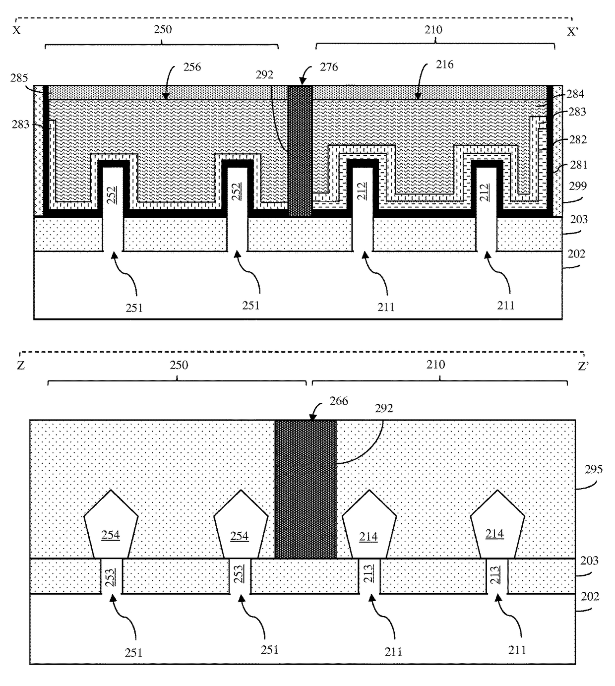
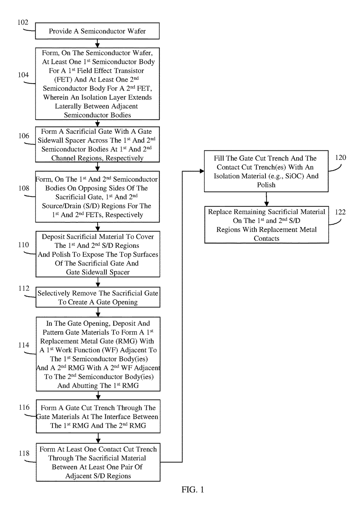
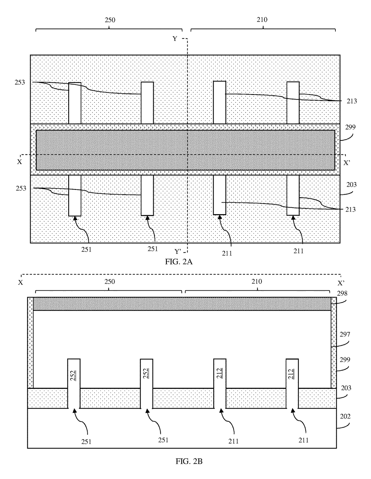
[0041]As mentioned above, the gate cut and contact cut isolation regions are typically formed at different process levels. For example, the gate cut isolation region is typically formed prior to RMG formation (e.g., at the polysilicon open chemical mechanical polishing (POC) process level) by: forming a gate cut trench, which divides a sacrificial gate into a first sacrificial gate and a second sacrificial gate and which extends vertically to the isolation layer in the area between the first semiconductor fin(s) and the second semiconductor fin(s); filling the gate cut trench with silicon nitride; and performing a chemical mechanical polishing (CMP) process. After the gate cut isolation region is formed, the first sacrificial gate and the second sacrificial gate are selectively removed and replaced with a first RMG and a second RMG, respectively. The contact cut isolation region is typically formed at the middle of the line (MOL) process level by: forming a contact cut trench, which...


PUM


Abstract

In a method for forming an integrated circuit (IC) structure, which incorporates multiple field effect transistors (FETs) with discrete replacement metal gates (RMGs) and replacement metal contacts (RMCs), gate cut trench(es) and contact cut trench(es) are formed at the same process level. These trench(es) are then filled at the same time with the same isolation material to form gate cut isolation region(s) for electrically isolating adjacent RMGs and contact cut isolation region(s) for electrically isolating adjacent RMCs, respectively. The selected isolation material can be a low-K isolation material for optimal performance. Furthermore, since the same process step is used to fill both types of trenches, only a single chemical mechanical polishing (CMP) process is needed to remove the isolation material from above the gate level, thereby minimizing gate height loss and process variation. Also disclosed herein is an IC structure formed according to the method.

Description

BACKGROUNDField of the Invention[0001]The present invention relates to integrated circuits (ICs) and, more particularly, to methods of forming an IC structure that incorporates multiple field effect transistors (e.g., fin-type field effect transistors (FINFETs)) with discrete replacement metal gates (RMGs) and contacts.Description of Related Art[0002]In integrated circuit (IC) design, cells (also referred to as library elements) typically represent a set of field effect transistors (FETs) (e.g., a set of fin-type field effect transistors (FINFETs)) and the interconnect structure(s) that connect those FETs. An exemplary cell can incorporate multiple parallel semiconductor bodies (e.g., semiconductor fins), including at least one first semiconductor body with a first channel region and first source / drain regions for at least one first FET with a first-type conductivity (e.g., a P-type FET) and at least one second semiconductor body with a second channel region and second source / drain ...

Claims


Application Information

Patent Timeline
IPC IPC(8): H01L21/28H01L29/49H01L27/088H01L21/8234H01L29/66H01L21/3105H01L21/762
CPCH01L27/0886H01L21/823481H01L21/823431H01L21/823468H01L21/823475H01L29/49H01L29/66545H01L21/31053H01L21/76229H01L21/28123H01L21/823437H01L21/823821H01L21/823828H01L21/823842H01L21/823878H01L29/7848H01L29/165H01L29/78651H01L21/823871
Inventor ZANG, HUIHUANG, HAIGOUQIU, XIAOFENG
Owner GLOBALFOUNDRIES US INC
Why Eureka
Try Eureka