Apparatus and algorithm for carrier profiling in scanning frequency comb microscopy

a scanning frequency comb microscopy and algorithm technology, applied in scanning probe microscopy, instruments, measurement devices, etc., can solve the problems of not only being able to apply deconvolution easily, but also being able to achieve finer effective radius, finer resolution, and avoiding calibration of instruments

Active Publication Date: 2018-03-27
HAGMANN MARK J
View PDF10 Cites 2 Cited by
  • Summary
  • Abstract
  • Description
  • Claims
  • Application Information

AI Technical Summary

Benefits of technology

[0022]The use of a MFC to measure spreading resistance can be further refined than as described in the '078 or '734 patent in a manner to eliminate the need for calibration of the instrument in regards to a given sample. The resultant methodology is also nondestructive to the sample, permits free scanning of the sample, provides a finer effective radius with a tunneling junction (and therefore provides finer resolution), and requires less intensive preparation of STM tips as compared to doped diamond tips utilized in prior art methods. The methodology of the present invention allows for this by measuring a power loss of the MFC at the tunneling junction as the current spreads out therefrom. Scanning across the sample is possible, in part, because the sample is not destroyed or otherwise altered when undergoing testing that utilizes a MFC. Carrier profiles may, therefore, be made on a local or a global scale by utilizing the methodology herein.
[0024]The new methodology allows for the non-destructive scanning of a semi-conductive sample while accounting for the effects of multiple mechanisms for power attenuation within the sample. Results are interpreted using a circuit model that accounts for these other mechanisms of attenuation in the semi-conductor in addition to the spreading resistance, to provide greater accuracy and finer resolution. Because the methodology is non-destructive and the impulse function is known, deconvolution is not only possible but easily applied. Finally, measurement of the power in the MFC at two points in the circuit allows for direct measurement of the attenuation.

Problems solved by technology

Because the methodology is non-destructive and the impulse function is known, deconvolution is not only possible but easily applied.

Method used


Image

  • Apparatus and algorithm for carrier profiling in scanning frequency comb microscopy
  • Apparatus and algorithm for carrier profiling in scanning frequency comb microscopy
  • Apparatus and algorithm for carrier profiling in scanning frequency comb microscopy

Examples


Embodiment Construction

[0039]With reference now to the drawings, the preferred embodiment of the method for carrier profiling and an apparatus for conducting the same is herein described. It should be noted that the articles “a”, “an”, and “the”, as used in this specification, include plural referents unless the content clearly dictates otherwise.

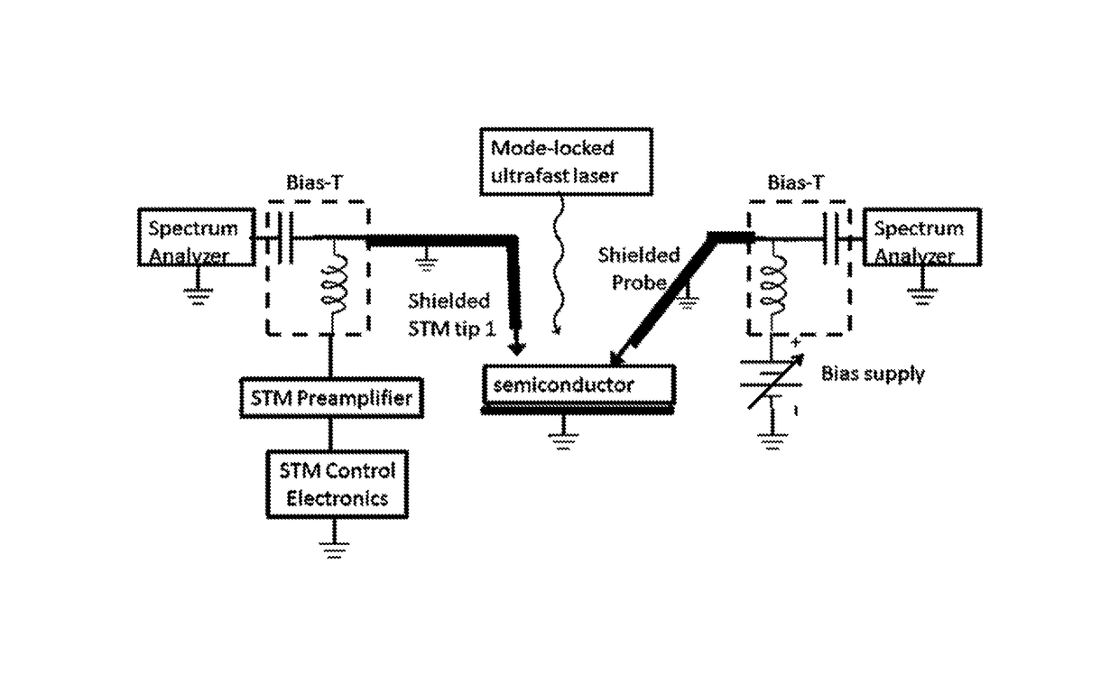
[0040]A microwave frequency comb (MFC) having hundreds of harmonics that set the present state-of-the-art for a narrow linewidth microwave source may be generated by focusing a mode-locked ultrafast laser on the tunneling junction of a scanning tunneling microscope (STM) [M. J. Hagmann, A. J. Taylor and D. A. Yarotski, “Observation of 200th harmonic with fractional linewidth of 10−10 in a microwave frequency comb generated in a tunneling junction,” Appl. Phys. Lett. 101, 241102 (2012)]. Quasi-periodic excitation of the tunneling junction by the laser superimposes a regular sequence of short (≈15 fs) current pulses on the DC tunneling current, and in the frequency...


PUM


Abstract

A semiconductor carrier profiling method utilizes a scanning tunneling microscope and shielded probe with an attached spectrum analyzer to measure power loss of a microwave frequency comb generated in a tunneling junction. From this power loss and by utilizing an equivalent circuit or other model, spreading resistance may be determined and carrier density from the spreading resistance. The methodology is non-destructive of the sample and allows scanning across the surface of the sample. By not being destructive, additional analysis methods, like deconvolution, are available for use.

Description

CROSS-REFERENCES TO RELATED APPLICATIONS[0001]The present invention claims priority as a non-provisional perfection of prior filed U.S. Application No. 62 / 305,619, filed Mar. 9, 2016, and incorporates the same by reference herein in its entirety.FIELD OF THE INVENTION[0002]The present invention is an apparatus and method for the carrier profiling of semiconductors, one that more specifically utilizes Scanning Frequency Comb Microscopy and measuring the spreading resistance in the semiconductor at a tunneling junction which has a sub-nanometer radius.BACKGROUND OF THE INVENTION[0003]The semiconductor industry is at a crisis because much finer resolution is required to meet their needs as they progress to the 10-nm, 7-nm, and finer lithography nodes to meet the demand for improved device performance. For example, while the chip capacity in flash memory increased by 100-fold from 2005 to 2013 the number of reliable state changes decreased at each step to finer lithography so the reliab...

Claims


Application Information

Patent Timeline
Patent Type & Authority Patents(United States)
IPC IPC(8): G01Q60/10G01Q10/04
CPCG01Q60/10G01Q10/04G01Q60/12
Inventor HAGMANN, MARK J.
Owner HAGMANN MARK J
Why Eureka
Try Eureka