CMOS input buffer with low supply current and voltage down shifting

a technology of input buffer and supply current, applied in the field of cmos input buffer, can solve the problems of unfavorable spikes at the output of the buffer, and achieve the effects of reducing the noise margin and reducing the noise of the input signal

Active Publication Date: 2018-04-03
NXP ISRAEL LTD
View PDF4 Cites 3 Cited by
  • Summary
  • Abstract
  • Description
  • Claims
  • Application Information

AI Technical Summary

Benefits of technology

[0011]For one embodiment of the invention, the target is to reduce the supply current consumption to the minimum possible, mostly for supporting applications where power consumption is a critical parameter. This goal is addressing both the cases where input voltage level is not forcing the input stage of the buffer to very deep near or sub-threshold levels for long time, when the input signal is switching, and when the input signal is noisy because of ringing.
[0012]Additionally, embodiments of the invention also include increase of the noise margin of the input signal, and mitigate the cases when input transition time is fairly long, and input signal is noisy during the transition. Such cases might cause undesired spikes at the output of the buffer.

Problems solved by technology

Such cases might cause undesired spikes at the output of the buffer.

Method used


Image

  • CMOS input buffer with low supply current and voltage down shifting
  • CMOS input buffer with low supply current and voltage down shifting
  • CMOS input buffer with low supply current and voltage down shifting

Examples


Embodiment Construction

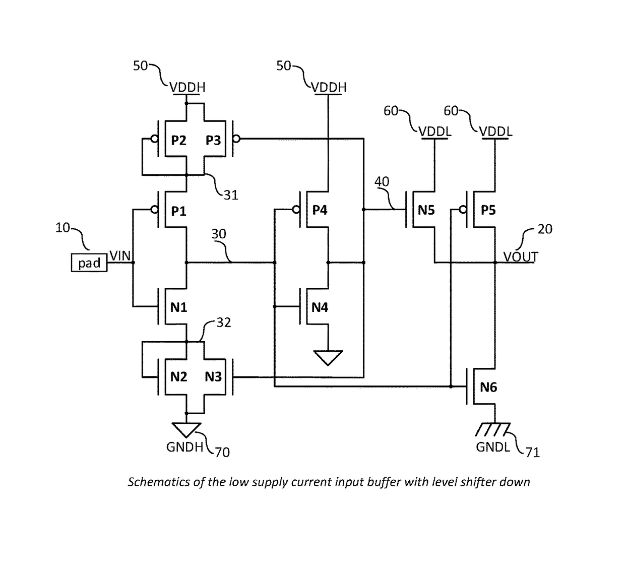
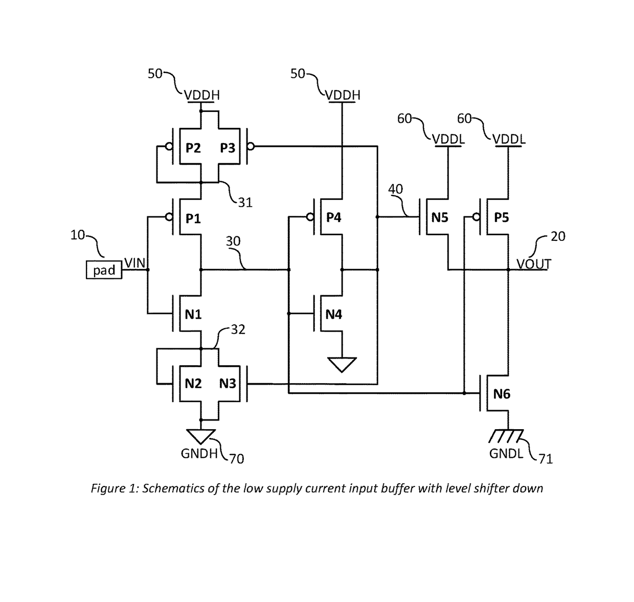
[0022]The present invention includes a method and apparatus for a low power CMOS input circuit typically connected to the bonding pads of input / output (I / O) pins of integrated circuits. It can be used either as a complete cell that performs the input buffering of signals entering the integrated circuit, or integrated in a more complex input / output circuit, such as bi-directional input / output buffer.

[0023]In the following description, numerous specific details are set forth. However, it is understood that embodiments of the invention may be practiced without these specific details. In other instances, well-known circuits, structures and techniques have not been shown in detail in order not to obscure the understanding of this description.

[0024]Reference throughout the specification to “one embodiment” or “an embodiment” means that a particular feature, structure, or characteristic described in connection with the embodiment is included in at least one embodiment of the present invent...


PUM


Abstract

A method for implementing a CMOS input buffer that consumes very low current even when input levels are less than full swing. An additional optional stage enables conversion to very low voltage swing. The circuit can be manufactured with a standard CMOS processing technology and with high immunity to variation of process parameters. The circuit provides some hysteresis response, enhancing the input voltage margin.

Description

FIELD OF THE INVENTION[0001]The invention relates to CMOS input buffer and more specific to low-power design of input buffers.BACKGROUND OF THE INVENTION[0002]The conventional circuit for input buffer for CMOS technology is based on conventional CMOS inverters, as presented in FIG. 2. In that circuit, NMOS transistor NC1 and PMOS transistor PC1 (as show in FIG. 2) act as input stage inverter, which is powered by VDDH supply (node 83 in FIG. 2), and provides output voltage levels of VDDH and GNDH (node 85 in FIG. 2). The second stage is a CMOS inverter, constructed by NMOS transistor NC2 and PMOS transistor PC2 (as show in FIG. 2), powered by VDDL supply (node 84 on FIG. 2), which is typically the same or lower voltage than VDDH. VDDL is typically equal to the core voltage of the integrated circuit. The input signal to this circuit is names VIN (node 80 on FIG. 2), and the output signal is named VOUT (node 82 on FIG. 2).[0003]The circuit in FIG. 2 has several disadvantages, which are...

Claims


Application Information

Patent Timeline
Patent Type & Authority Patents(United States)
IPC IPC(8): H03K19/0175H03K19/00H03K19/0185
CPCH03K19/018521H03K19/0013
Inventor LIRAN, TUVIAFELDMAN, NEILZANGI, UZI
Owner NXP ISRAEL LTD
Why Eureka
Try Eureka