Packaged semiconductor device having patterned conductance dual-material nanoparticle adhesion layer

Active Publication Date: 2018-04-10
TEXAS INSTR INC
View PDF65 Cites 1 Cited by
  • Summary
  • Abstract
  • Description
  • Claims
  • Application Information

AI Technical Summary

Benefits of technology

The patent describes a method for creating a layer on a substrate made of a first material with alternating zones of conductive and non-conductive nanoparticles. The method involves dispensing two solvent pastes onto the surface of the substrate using two nozzles, and then applying energy to the nanoparticles to sinter them and diffuse them into the substrate. The resulting layer consists of a sequence of conductive and non-conductive zones. This technique can create a layer with specific electrical properties and could have applications in electronics and sensors.

Problems solved by technology

Roughening of the leadframe surface may have some unwelcome side effects.
General roughening of the surface impacts wire bonding negatively.
For example, vision systems have trouble seeing the roughened surface, the rough surface shortens capillary life; and micro-contaminants on the rough surface degrade bonding consistency.
The resin bleed, in turn, can degrade moisture level sensitivity and interfere with down bonds on the chip pad.
The success of all these efforts has only been limited, especially because the adhesive effectiveness is diminishing ever more when another downscaling step of device miniaturization is implemented.

Method used


Image

  • Packaged semiconductor device having patterned conductance dual-material nanoparticle adhesion layer
  • Packaged semiconductor device having patterned conductance dual-material nanoparticle adhesion layer
  • Packaged semiconductor device having patterned conductance dual-material nanoparticle adhesion layer

Examples


Embodiment Construction

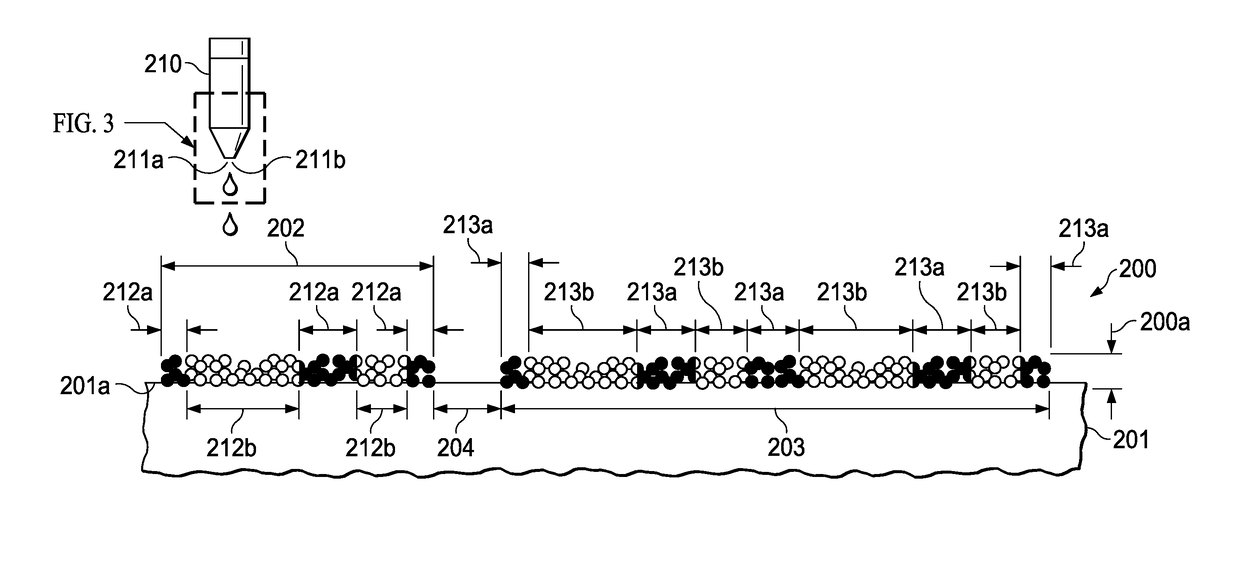
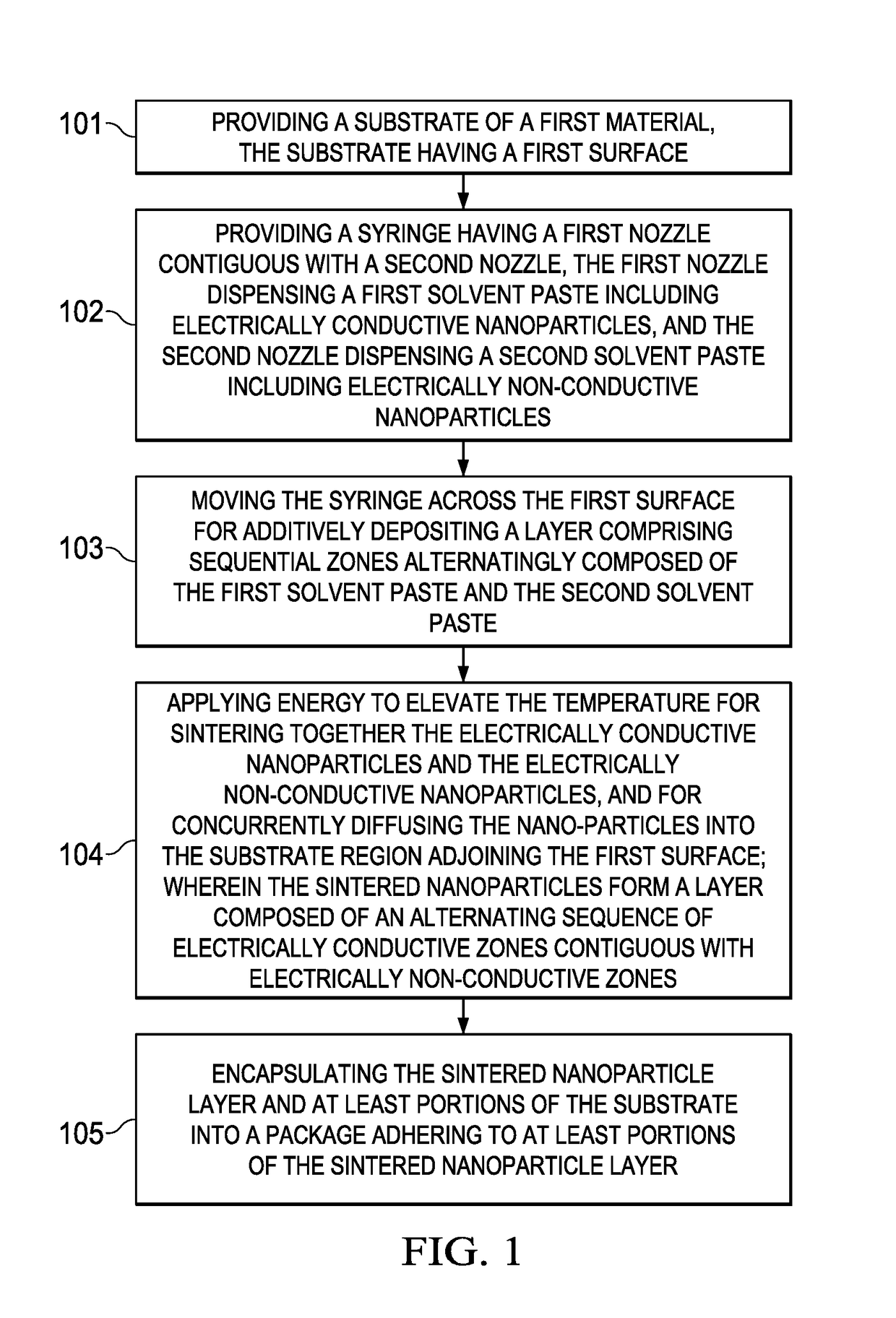
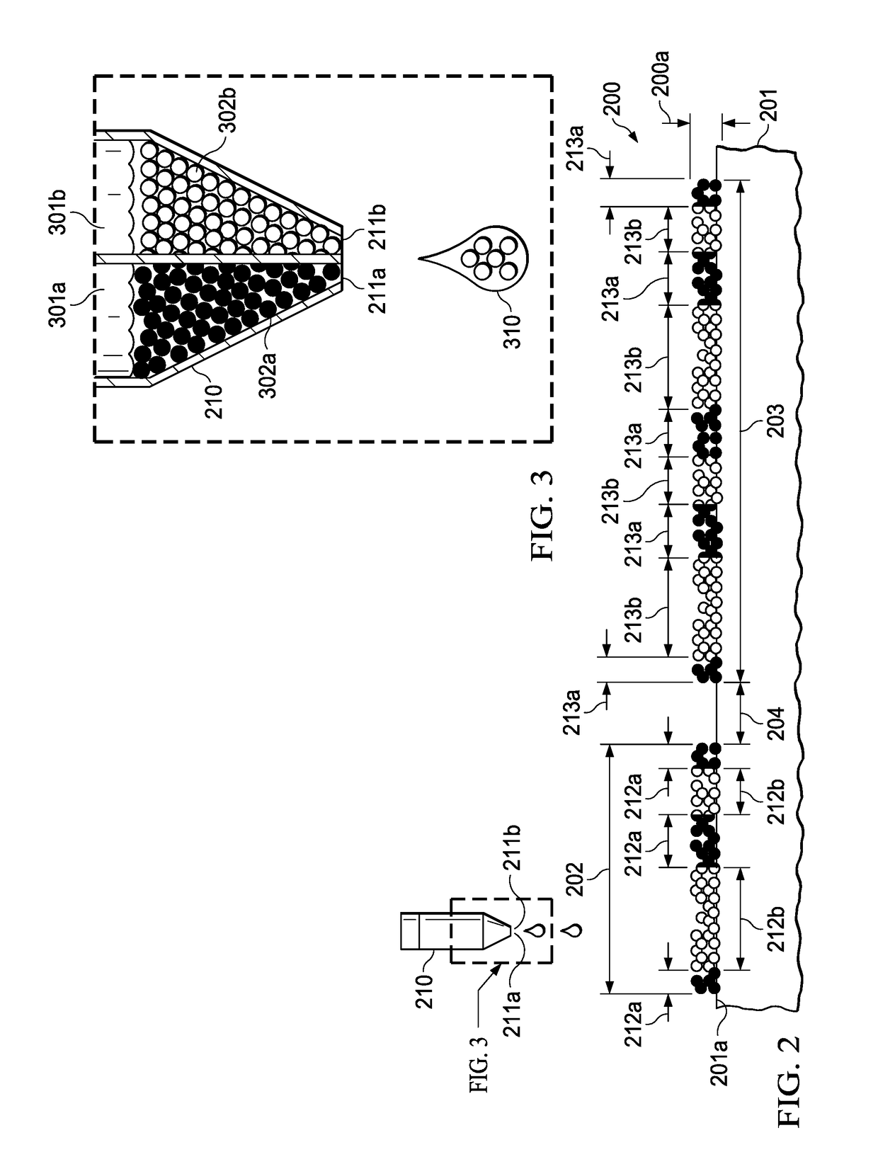
[0014]In an embodiment of the invention, a method for enhancing the adhesion and mechanical bonding between objects made of diverse materials such as metals and polymerics is described. The method comprises the formation and anchoring of an additive adhesion film composed of intermeshed nanoparticle layers between the objects. FIG. 1 is a diagram summarizing an embodiment of the invention. An object, onto which the additive film is constructed, is herein referred to as substrate, while another object, which needs adhesion to the substrate, is herein referred to as package. As examples, a substrate is denoted 201 in FIG. 2, and a package is denoted 501 in FIG. 5.

[0015]An application of the process flow shown in FIG. 1 can be applied to the fabrication technology of semiconductor devices. In semiconductor technology, the substrate typically is either a metallic leadframe or a laminated substrate composed of a plurality of alternating electrically insulating and electrically conductive...


PUM


Abstract

In an embodiment, a substrate made of a first material and having a surface is provided. A first and second nozzle dispense a first solvent paste including electrically conductive nanoparticles and a second solvent paste including non-conductive nanoparticles respectively while moving over the surface of the substrate. The first and second nozzles additively deposit a uniform layer comprising sequential and contiguous zones alternating between the first solvent paste and the second solvent paste. Energy is applied to the nanoparticles to sinter together the nanoparticles and diffuse the nanoparticles into the substrate. The sintered nanoparticles form a layer composed of an alternating sequence of electrically conductive zones contiguous with electrically non-conductive zones.

Description

FIELD[0001]Embodiments of the present invention are related in general to the field of semiconductor devices and processes, and more specifically to the structure and fabrication of packaged semiconductor devices having patterned conductance dual-material nanoparticle layers.DESCRIPTION OF RELATED ART[0002]Based on their functions, semiconductor packages include a variety of different materials. Metals formed as leadframes are employed for mechanical stability, and electrical and thermal conductance. Insulators, such as polymeric molding compounds, are used for encapsulations. In packaging fabrication, it is common practice to attach a plurality of semiconductor chips to a strip of leadframe (or packaging substrate), to connect the chips to their respective leads, and then to encapsulate the assembled chips in packages. Packages protect the enclosed parts against mechanical damage and environmental influences such as moisture and light. After the encapsulation step, the package chip...

Claims


Application Information

Patent Timeline
IPC IPC(8): H01L21/00H01L23/29H01L23/00H01L21/67H01L21/48H01L21/56H01L23/495
CPCH01L23/49586H01L24/48H01L23/49517H01L23/49558H01L23/49582H01L21/6715H01L21/67121H01L21/4825H01L21/4867H01L21/4857H01L21/56H01L23/293H01L2224/48091H01L2224/48245H01L2224/48465H01L2924/183H01L2924/186H01L24/16H01L2224/16245H01L2224/32245H01L2224/48247H01L2224/73265H01L2924/00014H01L2224/32225H01L2924/00
Inventor COOK, BENJAMIN STASSENLIN, DANIEL YONG
Owner TEXAS INSTR INC
Why Eureka
Try Eureka